DF2367VF33V Renesas Electronics America, DF2367VF33V Datasheet - Page 48
DF2367VF33V
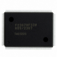
Manufacturer Part Number
DF2367VF33V
Description
IC H8S/2367 MCU FLASH 128QFP
Manufacturer
Renesas Electronics America
Series
H8® H8S/2300r
Datasheets
1.HEWH8E10A.pdf
(19 pages)
2.D12312SVTE25V.pdf
(341 pages)
3.DF2368VTE34V.pdf
(1044 pages)
Specifications of DF2367VF33V
Core Processor
H8S/2000
Core Size
16-Bit
Speed
33MHz
Connectivity
I²C, IrDA, SCI, SmartCard
Peripherals
DMA, POR, PWM, WDT
Number Of I /o
84
Program Memory Size
384KB (384K x 8)
Program Memory Type
FLASH
Ram Size
24K x 8
Voltage - Supply (vcc/vdd)
3 V ~ 3.6 V
Data Converters
A/D 10x10b, D/A 2x8b
Oscillator Type
Internal
Operating Temperature
-20°C ~ 75°C
Package / Case
128-QFP
For Use With
YR0K42378FC000BA - KIT EVAL FOR H8S/2378HS0005KCU11H - EMULATOR E10A-USB H8S(X),SH2(A)
Lead Free Status / RoHS Status
Lead free / RoHS Compliant
Eeprom Size
-
Available stocks
Company
Part Number
Manufacturer
Quantity
Price
Company:

Part Number:
DF2367VF33V
Manufacturer:
Renesas Electronics America
Quantity:
135
Company:
Part Number:
DF2367VF33V
Manufacturer:
Renesas Electronics America
Quantity:
10 000


Section 14 Serial Communication Interface (SCI, IrDA)
Figure 14.1 Block Diagram of SCI............................................................................................ 543
Figure 14.2 Data Format in Asynchronous Communication (Example with 8-Bit Data,
Figure 14.3 Receive Data Sampling Timing in Asynchronous Mode ....................................... 578
Figure 14.4 Relation between Output Clock and Transfer Data Phase
Figure 14.5 Sample SCI Initialization Flowchart ...................................................................... 580
Figure 14.6 Example of Operation in Transmission in Asynchronous Mode
Figure 14.7 Sample Serial Transmission Flowchart .................................................................. 583
Figure 14.8 Example of SCI Operation in Reception (Example with 8-Bit Data, Parity,
Figure 14.9 Sample Serial Reception Data Flowchart (1) ......................................................... 586
Figure 14.9 Sample Serial Reception Data Flowchart (2) ......................................................... 587
Figure 14.10 Example of Communication Using Multiprocessor Format
Figure 14.11 Sample Multiprocessor Serial Transmission Flowchart ......................................... 590
Figure 14.12 Example of SCI Operation in Reception (Example with 8-Bit Data,
Figure 14.13 Sample Multiprocessor Serial Reception Flowchart (1)......................................... 593
Figure 14.13 Sample Multiprocessor Serial Reception Flowchart (2)......................................... 594
Figure 14.14 Data Format in Clocked Synchronous Communication (For LSB-First) ............... 595
Figure 14.15 Sample SCI Initialization Flowchart ...................................................................... 596
Figure 14.16 Sample SCI Transmission Operation in Clocked Synchronous Mode ................... 598
Figure 14.17 Sample Serial Transmission Flowchart .................................................................. 599
Figure 14.18 Example of SCI Operation in Reception ................................................................ 600
Figure 14.19 Sample Serial Reception Flowchart ....................................................................... 601
Figure 14.20 Sample Flowchart of Simultaneous Serial Transmit and Receive Operations ....... 603
Figure 14.21 Schematic Diagram of Smart Card Interface Pin Connections............................... 604
Figure 14.22 Normal Smart Card Interface Data Format ............................................................ 605
Figure 14.23 Direct Convention (SDIR = SINV = O/E = 0) ....................................................... 605
Figure 14.24 Inverse Convention (SDIR = SINV = O/E = 1) ..................................................... 606
Figure 14.25 Receive Data Sampling Timing in Smart Card Mode
Figure 14.26 Retransfer Operation in SCI Transmit Mode ......................................................... 609
Figure 14.27 TEND Flag Generation Timing in Transmission Operation .................................. 610
Figure 14.28 Example of Transmission Processing Flow ........................................................... 611
Figure 14.29 Retransfer Operation in SCI Receive Mode ........................................................... 612
Figure 14.30 Example of Reception Processing Flow................................................................. 613
Rev.6.00 Mar. 18, 2009 Page xlvi of lviii
REJ09B0050-0600
Parity, Two Stop Bits)............................................................................................ 576
(Asynchronous Mode)............................................................................................ 579
(Example with 8-Bit Data, Parity, One Stop Bit) ................................................... 582
One Stop Bit).......................................................................................................... 584
(Transmission of Data H'AA to Receiving Station A) ........................................... 589
Multiprocessor Bit, One Stop Bit).......................................................................... 592
(Using Clock of 372 Times the Bit Rate) ............................................................... 607
Related parts for DF2367VF33V
Image
Part Number
Description
Manufacturer
Datasheet
Request
R

Part Number:
Description:
CONN PLUG 12POS DUAL 0.5MM SMD
Manufacturer:
Hirose Electric Co Ltd
Datasheet:
Part Number:
Description:
CONN PLUG 18POS DUAL 0.5MM SMD
Manufacturer:
Hirose Electric Co Ltd
Datasheet:
Part Number:
Description:
CONN PLUG 14POS DUAL 0.5MM SMD
Manufacturer:
Hirose Electric Co Ltd
Datasheet:
Part Number:
Description:
CONN RECEPT 20POS DUAL 0.5MM SMD
Manufacturer:
Hirose Electric Co Ltd
Datasheet:
Part Number:
Description:
CONN PLUG 16POS DUAL 0.5MM SMD
Manufacturer:
Hirose Electric Co Ltd
Datasheet:
Part Number:
Description:
CONN RECEPT 16POS DUAL 0.5MM SMD
Manufacturer:
Hirose Electric Co Ltd
Datasheet:
Part Number:
Description:
CONN PLUG 20POS DUAL 0.5MM SMD
Manufacturer:
Hirose Electric Co Ltd
Datasheet:
Part Number:
Description:
CONN PLUG 30POS DUAL 0.5MM SMD
Manufacturer:
Hirose Electric Co Ltd
Datasheet:
Part Number:
Description:
CONN RECEPT 30POS DUAL 0.5MM SMD
Manufacturer:
Hirose Electric Co Ltd
Datasheet:
Part Number:
Description:
CONN PLUG 40POS DUAL 0.5MM SMD
Manufacturer:
Hirose Electric Co Ltd
Datasheet:

Part Number:
Description:
KIT STARTER FOR M16C/29
Manufacturer:
Renesas Electronics America
Datasheet:

Part Number:
Description:
KIT STARTER FOR R8C/2D
Manufacturer:
Renesas Electronics America
Datasheet:

Part Number:
Description:
R0K33062P STARTER KIT
Manufacturer:
Renesas Electronics America
Datasheet:

Part Number:
Description:
KIT STARTER FOR R8C/23 E8A
Manufacturer:
Renesas Electronics America
Datasheet:

Part Number:
Description:
KIT STARTER FOR R8C/25
Manufacturer:
Renesas Electronics America
Datasheet: