DF2367VF33V Renesas Electronics America, DF2367VF33V Datasheet - Page 45
DF2367VF33V
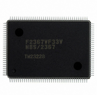
Manufacturer Part Number
DF2367VF33V
Description
IC H8S/2367 MCU FLASH 128QFP
Manufacturer
Renesas Electronics America
Series
H8® H8S/2300r
Datasheets
1.HEWH8E10A.pdf
(19 pages)
2.D12312SVTE25V.pdf
(341 pages)
3.DF2368VTE34V.pdf
(1044 pages)
Specifications of DF2367VF33V
Core Processor
H8S/2000
Core Size
16-Bit
Speed
33MHz
Connectivity
I²C, IrDA, SCI, SmartCard
Peripherals
DMA, POR, PWM, WDT
Number Of I /o
84
Program Memory Size
384KB (384K x 8)
Program Memory Type
FLASH
Ram Size
24K x 8
Voltage - Supply (vcc/vdd)
3 V ~ 3.6 V
Data Converters
A/D 10x10b, D/A 2x8b
Oscillator Type
Internal
Operating Temperature
-20°C ~ 75°C
Package / Case
128-QFP
For Use With
YR0K42378FC000BA - KIT EVAL FOR H8S/2378HS0005KCU11H - EMULATOR E10A-USB H8S(X),SH2(A)
Lead Free Status / RoHS Status
Lead free / RoHS Compliant
Eeprom Size
-
Available stocks
Company
Part Number
Manufacturer
Quantity
Price
Company:

Part Number:
DF2367VF33V
Manufacturer:
Renesas Electronics America
Quantity:
135
Company:
Part Number:
DF2367VF33V
Manufacturer:
Renesas Electronics America
Quantity:
10 000


Figure 7.30 Example of DREQ Pin Falling Edge Activated Single Address Mode Transfer.... 279
Figure 7.31 Example of DREQ Pin Low Level Activated Single Address Mode Transfer....... 280
Figure 7.32 Example of Dual Address Transfer Using Write Data Buffer Function................. 281
Figure 7.33 Example of Single Address Transfer Using Write Data Buffer Function .............. 282
Figure 7.34 Example of Multi-Channel Transfer ...................................................................... 283
Figure 7.35 Example of Procedure for Continuing Transfer on Channel Interrupted
Figure 7.36 Example of Procedure for Forcibly Terminating DMAC Operation...................... 285
Figure 7.37 Example of Procedure for Clearing Full Address Mode ........................................ 286
Figure 7.38 Block Diagram of Transfer End/Transfer Break Interrupt ..................................... 287
Figure 7.39 DMAC Register Update Timing ............................................................................ 288
Figure 7.40 Contention between DMAC Register Update and CPU Read................................ 289
Figure 7.41 Example in which Low Level is Not Output at TEND Pin .................................... 291
Section 8 Data Transfer Controller (DTC)
Figure 8.1
Figure 8.2
Figure 8.3
Figure 8.4
Figure 8.5
Figure 8.6
Figure 8.7
Figure 8.8
Figure 8.9
Figure 8.10 DTC Operation Timing (Example in Normal Mode or Repeat Mode)................... 313
Figure 8.11 DTC Operation Timing (Example of Block Transfer Mode,
Figure 8.12 DTC Operation Timing (Example of Chain Transfer) ........................................... 314
Figure 8.13 Chain Transfer when Counter = 0 .......................................................................... 319
Section 10 16-Bit Timer Pulse Unit (TPU)
Figure 10.1 Block Diagram of TPU........................................................................................... 404
Figure 10.2 Example of Counter Operation Setting Procedure ................................................. 439
Figure 10.3 Free-Running Counter Operation ........................................................................... 440
Figure 10.4 Periodic Counter Operation.................................................................................... 441
Figure 10.5 Example of Setting Procedure for Waveform Output by Compare Match............. 442
Figure 10.6 Example of 0 Output/1 Output Operation .............................................................. 443
Figure 10.7 Example of Toggle Output Operation .................................................................... 443
Figure 10.8 Example of Setting Procedure for Input Capture Operation................................... 444
Figure 10.9 Example of Input Capture Operation...................................................................... 445
by NMI Interrupt .................................................................................................... 284
Block Diagram of DTC .......................................................................................... 294
Block Diagram of DTC Activation Source Control ............................................... 302
Correspondence between DTC Vector Address and Register Information ............ 303
Correspondence between DTC Vector Address and Register Information ............ 303
Flowchart of DTC Operation.................................................................................. 307
Memory Mapping in Normal Mode ....................................................................... 309
Memory Mapping in Repeat Mode ........................................................................ 310
Memory Mapping in Block Transfer Mode ........................................................... 311
Operation of Chain Transfer................................................................................... 312
with Block Size of 2).............................................................................................. 313
Rev.6.00 Mar. 18, 2009 Page xliii of lviii
REJ09B0050-0600
Related parts for DF2367VF33V
Image
Part Number
Description
Manufacturer
Datasheet
Request
R

Part Number:
Description:
CONN PLUG 12POS DUAL 0.5MM SMD
Manufacturer:
Hirose Electric Co Ltd
Datasheet:
Part Number:
Description:
CONN PLUG 18POS DUAL 0.5MM SMD
Manufacturer:
Hirose Electric Co Ltd
Datasheet:
Part Number:
Description:
CONN PLUG 14POS DUAL 0.5MM SMD
Manufacturer:
Hirose Electric Co Ltd
Datasheet:
Part Number:
Description:
CONN RECEPT 20POS DUAL 0.5MM SMD
Manufacturer:
Hirose Electric Co Ltd
Datasheet:
Part Number:
Description:
CONN PLUG 16POS DUAL 0.5MM SMD
Manufacturer:
Hirose Electric Co Ltd
Datasheet:
Part Number:
Description:
CONN RECEPT 16POS DUAL 0.5MM SMD
Manufacturer:
Hirose Electric Co Ltd
Datasheet:
Part Number:
Description:
CONN PLUG 20POS DUAL 0.5MM SMD
Manufacturer:
Hirose Electric Co Ltd
Datasheet:
Part Number:
Description:
CONN PLUG 30POS DUAL 0.5MM SMD
Manufacturer:
Hirose Electric Co Ltd
Datasheet:
Part Number:
Description:
CONN RECEPT 30POS DUAL 0.5MM SMD
Manufacturer:
Hirose Electric Co Ltd
Datasheet:
Part Number:
Description:
CONN PLUG 40POS DUAL 0.5MM SMD
Manufacturer:
Hirose Electric Co Ltd
Datasheet:

Part Number:
Description:
KIT STARTER FOR M16C/29
Manufacturer:
Renesas Electronics America
Datasheet:

Part Number:
Description:
KIT STARTER FOR R8C/2D
Manufacturer:
Renesas Electronics America
Datasheet:

Part Number:
Description:
R0K33062P STARTER KIT
Manufacturer:
Renesas Electronics America
Datasheet:

Part Number:
Description:
KIT STARTER FOR R8C/23 E8A
Manufacturer:
Renesas Electronics America
Datasheet:

Part Number:
Description:
KIT STARTER FOR R8C/25
Manufacturer:
Renesas Electronics America
Datasheet: