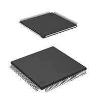
DF2161BVTE10 Renesas Electronics America, DF2161BVTE10 Datasheet - Page 544

DF2161BVTE10
Manufacturer Part Number
DF2161BVTE10
Description
MCU 3V 128K 144-TQFP
Manufacturer
Renesas Electronics America
Series
H8® H8S/2100r
Datasheet
1.DF2160BVT10V.pdf
(847 pages)
Specifications of DF2161BVTE10
Core Processor
H8S/2000
Core Size
16-Bit
Speed
10MHz
Connectivity
Host Interface (LPC), I²C, IrDA, SCI, X-Bus
Peripherals
PWM, WDT
Number Of I /o
114
Program Memory Size
128KB (128K x 8)
Program Memory Type
FLASH
Ram Size
4K x 8
Voltage - Supply (vcc/vdd)
2.7 V ~ 3.6 V
Data Converters
A/D 8x10b; D/A 2x8b
Oscillator Type
Internal
Operating Temperature
-20°C ~ 75°C
Package / Case
144-TQFP, 144-VQFP
Lead Free Status / RoHS Status
Contains lead / RoHS non-compliant
Eeprom Size
-
Other names
HD64F2161BVTE10
HD64F2161BVTE10
HD64F2161BVTE10
- Current page: 544 of 847
- Download datasheet (5Mb)
Section 16 I
15. Note on ICDR read in transmit mode and ICDR write in receive mode
16. Note on ACKE and TRS bits in slave mode
16.6.1
The IIC operation can be enabled or disabled using the module stop control register. The initial
setting is for the IIC operation to be halted. Register access is enabled by canceling module stop
mode. For details, refer to section 26, Power-Down Modes.
Rev. 3.00 Mar 21, 2006 page 488 of 788
REJ09B0300-0300
(c) To confirm that the bus was not entered to the busy state while the MST bit is being set,
If ICDR is read in transmit mode (TRS = 1) or ICDR is written to in receive mode (TRS = 0),
the SCL pin may not be held low in some cases after transmit/receive operation has been
completed, thus inconveniently allowing clock pulses to be output on the SCL bus line before
ICDR is accessed correctly. To access ICDR correctly, read ICDR after setting receive mode
or write to ICDR after setting transmit mode.
In the I
mode (TRS = 1) and then the address is received in slave mode without performing appropriate
processing, interrupt handling may start at the rising edge of the 9th clock pulse even when the
address does not match. Similarly, if the start condition or address is transmitted from the
master device in slave transmit mode (TRS = 1), the IRIC flag may be set after the ICDRE flag
is set and 1 received as the acknowledge bit value (ACKB = 1), thus causing an interrupt
source even when the address does not match.
To use the I
A. When having received 1 as the acknowledge bit value for the last transmit data at the end
B. Set receive mode (TRS = 0) before the next start condition is input in slave mode.
check that the BBSY flag in the ICCR register is 0 immediately after the MST bit has been
set.
of a series of transmit operation, clear the ACKE bit in ICCR once to initialize the ACKB
bit to 0.
Complete transmit operation by the procedure shown in figure 16.24, in order to switch
from slave transmit mode to slave receive mode.
Module Stop Mode Setting
2
C bus interface, if 1 is received as the acknowledge bit value (ACKB = 1) in transmit
2
C Bus Interface (IIC) (Optional)
2
C bus interface module in slave mode, be sure to follow the procedures below.
Related parts for DF2161BVTE10
Image
Part Number
Description
Manufacturer
Datasheet
Request
R

Part Number:
Description:
KIT STARTER FOR M16C/29
Manufacturer:
Renesas Electronics America
Datasheet:

Part Number:
Description:
KIT STARTER FOR R8C/2D
Manufacturer:
Renesas Electronics America
Datasheet:

Part Number:
Description:
R0K33062P STARTER KIT
Manufacturer:
Renesas Electronics America
Datasheet:

Part Number:
Description:
KIT STARTER FOR R8C/23 E8A
Manufacturer:
Renesas Electronics America
Datasheet:

Part Number:
Description:
KIT STARTER FOR R8C/25
Manufacturer:
Renesas Electronics America
Datasheet:

Part Number:
Description:
KIT STARTER H8S2456 SHARPE DSPLY
Manufacturer:
Renesas Electronics America
Datasheet:

Part Number:
Description:
KIT STARTER FOR R8C38C
Manufacturer:
Renesas Electronics America
Datasheet:

Part Number:
Description:
KIT STARTER FOR R8C35C
Manufacturer:
Renesas Electronics America
Datasheet:

Part Number:
Description:
KIT STARTER FOR R8CL3AC+LCD APPS
Manufacturer:
Renesas Electronics America
Datasheet:

Part Number:
Description:
KIT STARTER FOR RX610
Manufacturer:
Renesas Electronics America
Datasheet:

Part Number:
Description:
KIT STARTER FOR R32C/118
Manufacturer:
Renesas Electronics America
Datasheet:

Part Number:
Description:
KIT DEV RSK-R8C/26-29
Manufacturer:
Renesas Electronics America
Datasheet:

Part Number:
Description:
KIT STARTER FOR SH7124
Manufacturer:
Renesas Electronics America
Datasheet:

Part Number:
Description:
KIT STARTER FOR H8SX/1622
Manufacturer:
Renesas Electronics America
Datasheet:

Part Number:
Description:
KIT DEV FOR SH7203
Manufacturer:
Renesas Electronics America
Datasheet:


