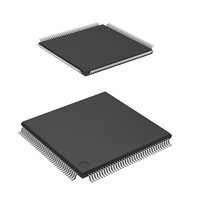
DF2161BVTE10 Renesas Electronics America, DF2161BVTE10 Datasheet - Page 43

DF2161BVTE10
Manufacturer Part Number
DF2161BVTE10
Description
MCU 3V 128K 144-TQFP
Manufacturer
Renesas Electronics America
Series
H8® H8S/2100r
Datasheet
1.DF2160BVT10V.pdf
(847 pages)
Specifications of DF2161BVTE10
Core Processor
H8S/2000
Core Size
16-Bit
Speed
10MHz
Connectivity
Host Interface (LPC), I²C, IrDA, SCI, X-Bus
Peripherals
PWM, WDT
Number Of I /o
114
Program Memory Size
128KB (128K x 8)
Program Memory Type
FLASH
Ram Size
4K x 8
Voltage - Supply (vcc/vdd)
2.7 V ~ 3.6 V
Data Converters
A/D 8x10b; D/A 2x8b
Oscillator Type
Internal
Operating Temperature
-20°C ~ 75°C
Package / Case
144-TQFP, 144-VQFP
Lead Free Status / RoHS Status
Contains lead / RoHS non-compliant
Eeprom Size
-
Other names
HD64F2161BVTE10
HD64F2161BVTE10
HD64F2161BVTE10
- Current page: 43 of 847
- Download datasheet (5Mb)
Figure 11.19 Conflict between OCR Write and Compare-Match
Figure 11.20 Conflict between OCRAR/OCRAF Write and Compare-Match
Section 12 8-Bit Timer (TMR)
Figure 12.1
Figure 12.2
Figure 12.3
Figure 12.4
Figure 12.5
Figure 12.6
Figure 12.7
Figure 12.8
Figure 12.9
Figure 12.10 Timing of OVF Flag Setting ................................................................................ 305
Figure 12.11 Timing of Input Capture Operation ..................................................................... 307
Figure 12.12 Timing of Input Capture Signal (Input Capture Signal Is Input during TICRR
Figure 12.13 Input Capture Signal Selection ............................................................................ 308
Figure 12.14 Conflict between TCNT Write and Clear ............................................................ 310
Figure 12.15 Conflict between TCNT Write and Increment..................................................... 311
Figure 12.16 Conflict between TCOR Write and Compare-Match........................................... 312
Section 13 Timer Connection
Figure 13.1
Figure 13.2
Figure 13.3
Figure 13.4
Figure 13.5
Figure 13.6
Figure 13.7
Figure 13.8
Figure 13.9
Section 14 Watchdog Timer (WDT)
Figure 14.1
Figure 14.2
Figure 14.3
Figure 14.4
(When Automatic Addition Function Is Not Used) ............................................. 282
(When Automatic Addition Function Is Used) .................................................... 283
Block Diagram of 8-Bit Timers (TMR_0 and TMR_1)....................................... 288
Block Diagram of 8-Bit Timers (TMR_Y and TMR_X) ..................................... 289
Pulse Output Example.......................................................................................... 301
Count Timing for Internal Clock Input ................................................................ 302
Count Timing for External Clock Input (Both Edges) ......................................... 302
Timing of CMF Setting at Compare-Match......................................................... 303
Timing of Toggled Timer Output by Compare-Match A Signal ......................... 303
Timing of Counter Clear by Compare-Match ...................................................... 304
Timing of Counter Clear by External Reset Input ............................................... 304
and TICRF Read)................................................................................................. 307
Block Diagram of Timer Connection................................................................... 318
Timing Chart for PWM Decoding ....................................................................... 330
Timing Chart for Clamp Waveform Generation (CL1 and CL2 Signals)............ 331
Timing Chart for Clamp Waveform Generation (CL3 Signal) ............................ 331
Timing Chart for Measurement of IVI Signal and IHI Signal Divided
Waveform Periods ............................................................................................... 334
2fH Modification Timing Chart........................................................................... 335
Fall Modification and IHI Synchronization Timing Chart................................... 337
IVG Signal/IHG Signal/CL4 Signal Timing Chart .............................................. 340
CBLANK Output Waveform Generation ............................................................ 343
Block Diagram of WDT....................................................................................... 346
Watchdog Timer Mode (RST/NMI = 1) Operation ............................................. 353
Interval Timer Mode Operation ........................................................................... 354
OVF Flag Set Timing........................................................................................... 354
Rev. 3.00 Mar 21, 2006 page xli of liv
Related parts for DF2161BVTE10
Image
Part Number
Description
Manufacturer
Datasheet
Request
R

Part Number:
Description:
KIT STARTER FOR M16C/29
Manufacturer:
Renesas Electronics America
Datasheet:

Part Number:
Description:
KIT STARTER FOR R8C/2D
Manufacturer:
Renesas Electronics America
Datasheet:

Part Number:
Description:
R0K33062P STARTER KIT
Manufacturer:
Renesas Electronics America
Datasheet:

Part Number:
Description:
KIT STARTER FOR R8C/23 E8A
Manufacturer:
Renesas Electronics America
Datasheet:

Part Number:
Description:
KIT STARTER FOR R8C/25
Manufacturer:
Renesas Electronics America
Datasheet:

Part Number:
Description:
KIT STARTER H8S2456 SHARPE DSPLY
Manufacturer:
Renesas Electronics America
Datasheet:

Part Number:
Description:
KIT STARTER FOR R8C38C
Manufacturer:
Renesas Electronics America
Datasheet:

Part Number:
Description:
KIT STARTER FOR R8C35C
Manufacturer:
Renesas Electronics America
Datasheet:

Part Number:
Description:
KIT STARTER FOR R8CL3AC+LCD APPS
Manufacturer:
Renesas Electronics America
Datasheet:

Part Number:
Description:
KIT STARTER FOR RX610
Manufacturer:
Renesas Electronics America
Datasheet:

Part Number:
Description:
KIT STARTER FOR R32C/118
Manufacturer:
Renesas Electronics America
Datasheet:

Part Number:
Description:
KIT DEV RSK-R8C/26-29
Manufacturer:
Renesas Electronics America
Datasheet:

Part Number:
Description:
KIT STARTER FOR SH7124
Manufacturer:
Renesas Electronics America
Datasheet:

Part Number:
Description:
KIT STARTER FOR H8SX/1622
Manufacturer:
Renesas Electronics America
Datasheet:

Part Number:
Description:
KIT DEV FOR SH7203
Manufacturer:
Renesas Electronics America
Datasheet:


