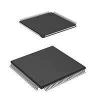
DF2161BVTE10 Renesas Electronics America, DF2161BVTE10 Datasheet - Page 414

DF2161BVTE10
Manufacturer Part Number
DF2161BVTE10
Description
MCU 3V 128K 144-TQFP
Manufacturer
Renesas Electronics America
Series
H8® H8S/2100r
Datasheet
1.DF2160BVT10V.pdf
(847 pages)
Specifications of DF2161BVTE10
Core Processor
H8S/2000
Core Size
16-Bit
Speed
10MHz
Connectivity
Host Interface (LPC), I²C, IrDA, SCI, X-Bus
Peripherals
PWM, WDT
Number Of I /o
114
Program Memory Size
128KB (128K x 8)
Program Memory Type
FLASH
Ram Size
4K x 8
Voltage - Supply (vcc/vdd)
2.7 V ~ 3.6 V
Data Converters
A/D 8x10b; D/A 2x8b
Oscillator Type
Internal
Operating Temperature
-20°C ~ 75°C
Package / Case
144-TQFP, 144-VQFP
Lead Free Status / RoHS Status
Contains lead / RoHS non-compliant
Eeprom Size
-
Other names
HD64F2161BVTE10
HD64F2161BVTE10
HD64F2161BVTE10
- Current page: 414 of 847
- Download datasheet (5Mb)
Section 14 Watchdog Timer (WDT)
14.6.5
Inputting the RESO output signal to the RESO pin of this LSI prevents the LSI from being
initialized correctly; the RESO signal must not be logically connected to the RES pin of the LSI.
To reset the entire system by the RESO signal, use the circuit as shown in figure 14.8.
14.6.6
When WDT_1 is used as a clock counter and is allowed to transit between high-speed mode and
sub-active or watch mode, the counter does not display the correct value due to internal clock
switching.
Specifically, when transiting from high-speed mode to sub-active or watch mode, that is, when the
control clock for WDT_1 switches from the main clock to the sub-clock, the counter incrementing
timing is delayed for approximately two to three clock cycles.
Similarly, when transiting from sub-active or watch mode to high-speed mode, the clock is not
supplied until stabilized internal oscillation is available because the main clock oscillator is halted
in sub-clock mode. The counter is therefore prevented from incrementing for the time specified by
the STS2 to STS0 bits in SBYCR after internal oscillation starts, thus producing counter value
differences for this time.
Special care must be taken when using WDT_1 as a clock counter. Note that no counter value
difference is produced while operated in the same mode.
Rev. 3.00 Mar 21, 2006 page 358 of 788
REJ09B0300-0300
System Reset by RESO
Counter Values during Transitions between High-Speed, Sub-Active, and Watch
Modes
Figure 14.8 Sample Circuit for Resetting System by RESO
Reset signal for entire system
RESO Signal
RESO
RESO
Reset input
RESO Signal
RESO
RESO
RESO
RES
This LSI
Related parts for DF2161BVTE10
Image
Part Number
Description
Manufacturer
Datasheet
Request
R

Part Number:
Description:
KIT STARTER FOR M16C/29
Manufacturer:
Renesas Electronics America
Datasheet:

Part Number:
Description:
KIT STARTER FOR R8C/2D
Manufacturer:
Renesas Electronics America
Datasheet:

Part Number:
Description:
R0K33062P STARTER KIT
Manufacturer:
Renesas Electronics America
Datasheet:

Part Number:
Description:
KIT STARTER FOR R8C/23 E8A
Manufacturer:
Renesas Electronics America
Datasheet:

Part Number:
Description:
KIT STARTER FOR R8C/25
Manufacturer:
Renesas Electronics America
Datasheet:

Part Number:
Description:
KIT STARTER H8S2456 SHARPE DSPLY
Manufacturer:
Renesas Electronics America
Datasheet:

Part Number:
Description:
KIT STARTER FOR R8C38C
Manufacturer:
Renesas Electronics America
Datasheet:

Part Number:
Description:
KIT STARTER FOR R8C35C
Manufacturer:
Renesas Electronics America
Datasheet:

Part Number:
Description:
KIT STARTER FOR R8CL3AC+LCD APPS
Manufacturer:
Renesas Electronics America
Datasheet:

Part Number:
Description:
KIT STARTER FOR RX610
Manufacturer:
Renesas Electronics America
Datasheet:

Part Number:
Description:
KIT STARTER FOR R32C/118
Manufacturer:
Renesas Electronics America
Datasheet:

Part Number:
Description:
KIT DEV RSK-R8C/26-29
Manufacturer:
Renesas Electronics America
Datasheet:

Part Number:
Description:
KIT STARTER FOR SH7124
Manufacturer:
Renesas Electronics America
Datasheet:

Part Number:
Description:
KIT STARTER FOR H8SX/1622
Manufacturer:
Renesas Electronics America
Datasheet:

Part Number:
Description:
KIT DEV FOR SH7203
Manufacturer:
Renesas Electronics America
Datasheet:


