HD64F2218TF24 Renesas Electronics America, HD64F2218TF24 Datasheet - Page 525
HD64F2218TF24
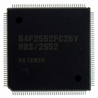
Manufacturer Part Number
HD64F2218TF24
Description
IC H8S MCU FLASH 128K 100-TQFP
Manufacturer
Renesas Electronics America
Series
H8® H8S/2200r
Specifications of HD64F2218TF24
Core Processor
H8S/2000
Core Size
16-Bit
Speed
24MHz
Connectivity
SCI, SmartCard, USB
Peripherals
DMA, POR, PWM, WDT
Number Of I /o
69
Program Memory Size
128KB (128K x 8)
Program Memory Type
FLASH
Ram Size
12K x 8
Voltage - Supply (vcc/vdd)
2.7 V ~ 3.6 V
Data Converters
A/D 6x10b
Oscillator Type
Internal
Operating Temperature
-20°C ~ 75°C
Package / Case
100-TQFP, 100-VQFP
For Use With
3DK2218-SS - KIT DEV H8S/2218 WINDOWS SIDESHW
Lead Free Status / RoHS Status
Contains lead / RoHS non-compliant
Eeprom Size
-


Bit
5
4
3
2
Bit Name
UCKS3
UCKS2
UCKS1
UCKS0
Initial Value R/W
0
R/W
Description
USB Operation Clock Select 3 to 0
These bits control the on-chip PLL, which generates
the USB operation clock (48 MHz). When UCKS3 to
UCKS0 are 0000, the PLL circuit stops and thus the
USB operation clock must be selected according to
the clock source.
The on-chip PLL circuit starts operating after the USB
module stop 2 bit has been cancelled. In addition, the
USB operation clock is supplied to the UDC core after
the USB operating clock stabilization time has been
passed. The completion timing of the USB operating
clock stabilization time can be detected by the
CK48READY flag in UIFR3.
UCKS0 to UCKS3 muse be written while the USB
module stop 2 bit (MSTPB0) is 1.
0000: USB operation clock stops (PLL stops)
0001: Reserved
001×: Reserved
010×: Reserved
0110: Uses a clock (48 MHz) generated by doubling
0111: Uses a clock (48 MHz) generated by tripling the
1×××: Reserved
The USB operating clock stabilization time is 2 ms.
Legend:
×: Don't care
the 24-MHz main oscillation by the PLL.
16-MHz main oscillation by the PLL.
Rev.7.00 Dec. 24, 2008 Page 469 of 698
REJ09B0074-0700
Related parts for HD64F2218TF24
Image
Part Number
Description
Manufacturer
Datasheet
Request
R


Part Number:
Description:
KIT STARTER FOR M16C/29
Manufacturer:
Renesas Electronics America
Datasheet:

Part Number:
Description:
KIT STARTER FOR R8C/2D
Manufacturer:
Renesas Electronics America
Datasheet:

Part Number:
Description:
R0K33062P STARTER KIT
Manufacturer:
Renesas Electronics America
Datasheet:

Part Number:
Description:
KIT STARTER FOR R8C/23 E8A
Manufacturer:
Renesas Electronics America
Datasheet:

Part Number:
Description:
KIT STARTER FOR R8C/25
Manufacturer:
Renesas Electronics America
Datasheet:

Part Number:
Description:
KIT STARTER H8S2456 SHARPE DSPLY
Manufacturer:
Renesas Electronics America
Datasheet:

Part Number:
Description:
KIT STARTER FOR R8C38C
Manufacturer:
Renesas Electronics America
Datasheet:

Part Number:
Description:
KIT STARTER FOR R8C35C
Manufacturer:
Renesas Electronics America
Datasheet:

Part Number:
Description:
KIT STARTER FOR R8CL3AC+LCD APPS
Manufacturer:
Renesas Electronics America
Datasheet:
Part Number:
Description:
KIT STARTER FOR RX610
Manufacturer:
Renesas Electronics America
Datasheet:

Part Number:
Description:
KIT STARTER FOR R32C/118
Manufacturer:
Renesas Electronics America
Datasheet:

Part Number:
Description:
KIT DEV RSK-R8C/26-29
Manufacturer:
Renesas Electronics America
Datasheet:

Part Number:
Description:
KIT STARTER FOR SH7124
Manufacturer:
Renesas Electronics America
Datasheet:

Part Number:
Description:
KIT STARTER FOR H8SX/1622
Manufacturer:
Renesas Electronics America
Datasheet: