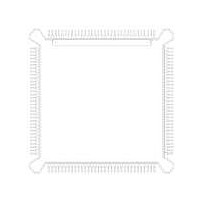
MC68HC16Z1CEH16 Freescale Semiconductor, MC68HC16Z1CEH16 Datasheet - Page 172

MC68HC16Z1CEH16
Manufacturer Part Number
MC68HC16Z1CEH16
Description
IC MCU 16BIT 16MHZ 132-PQFP
Manufacturer
Freescale Semiconductor
Series
HC16r
Specifications of MC68HC16Z1CEH16
Core Processor
CPU16
Core Size
16-Bit
Speed
16MHz
Connectivity
EBI/EMI, SCI, SPI
Peripherals
POR, PWM, WDT
Number Of I /o
16
Program Memory Type
ROMless
Ram Size
1K x 8
Voltage - Supply (vcc/vdd)
2.7 V ~ 5.5 V
Data Converters
A/D 8x10b
Oscillator Type
Internal
Operating Temperature
-40°C ~ 85°C
Package / Case
132-QFP
Processor Series
HC16Z
Core
CPU16
Data Bus Width
16 bit
Controller Family/series
68HC16
No. Of I/o's
26
Ram Memory Size
1KB
Cpu Speed
16MHz
No. Of Timers
2
Embedded Interface Type
QSPI, SCI
Rohs Compliant
Yes
Package
132PQFP
Family Name
HC16
Maximum Speed
16 MHz
Operating Supply Voltage
3.3|5 V
Number Of Programmable I/os
16
On-chip Adc
8-chx10-bit
Number Of Timers
11
Data Ram Size
1 KB
Interface Type
SCI, SPI, UART
Maximum Clock Frequency
16 MHz
Maximum Operating Temperature
+ 85 C
Mounting Style
SMD/SMT
Minimum Operating Temperature
- 40 C
Lead Free Status / RoHS Status
Lead free / RoHS Compliant
Eeprom Size
-
Program Memory Size
-
Lead Free Status / Rohs Status
Lead free / RoHS Compliant
Available stocks
Company
Part Number
Manufacturer
Quantity
Price
Company:
Part Number:
MC68HC16Z1CEH16
Manufacturer:
Freescale Semiconductor
Quantity:
10 000
Part Number:
MC68HC16Z1CEH16
Manufacturer:
FREESCALE
Quantity:
20 000
- Current page: 172 of 500
- Download datasheet (6Mb)
5.9.1.3 Chip-Select Option Registers
5-66
The chip-select address compare logic uses only the most significant bits to match an
address within a block. The value of the base address must be an integer multiple of
the block size.
Because the logic state of ADDR[23:20] follows that of ADDR19 in the CPU16, maxi-
mum block size is 512 Kbytes, and addresses from $080000 to $F7FFFF are inacces-
sible.
After reset, the MCU fetches the initialization routine from the address contained in the
reset vector, located beginning at address $000000 of program space. To support
bootstrap operation from reset, the base address field in the boot chip-select base ad-
dress register (CSBARBT) has a reset value of $000, which corresponds to a base ad-
dress of $000000 and a block size of 512 Kbytes. A memory device containing the
reset vector and initialization routine can be automatically enabled by CSBOOT after
a reset. Refer to
Option register fields determine timing of and conditions for assertion of chip-select
signals. To assert a chip-select signal, and to provide DSACK or autovector support,
other constraints set by fields in the option register and in the base address register
must also be satisfied. The following paragraphs summarize option register functions.
Refer to
The MODE bit determines whether chip-select assertion simulates an asynchronous
bus cycle, or is synchronized to the M6800-type bus clock signal ECLK available on
ADDR23. Refer to
BYTE[1:0] controls bus allocation for chip-select transfers. Port size, set when a chip-
select is enabled by a pin assignment register, affects signal assertion. When an 8-bit
port is assigned, any BYTE field value other than %00 enables the chip-select signal.
When a 16-bit port is assigned, however, BYTE field value determines when the chip-
select is enabled. The BYTE fields for CS[10:0] are cleared during reset. However,
both bits in the boot ROM chip-select option register (CSORBT) BYTE field are set
(%11) when the RESET signal is released.
R/W[1:0] causes a chip-select signal to be asserted only for a read, only for a write, or
for both read and write. Use this field in conjunction with the STRB bit to generate
asynchronous control signals for external devices.
The STRB bit controls the timing of a chip-select assertion in asynchronous mode. Se-
lecting address strobe causes a chip-select signal to be asserted synchronized with
the address strobe. Selecting data strobe causes a chip-select signal to be asserted
synchronized with the data strobe. This bit has no effect in synchronous mode.
DSACK[3:0] specifies the source of DSACK in asynchronous mode. It also allows the
user to optimize bus speed in a particular application by controlling the number of wait
states that are inserted.
D.2.21 Chip-Select Option Registers
5.9.4 Chip-Select Reset Operation
5.3 System Clock
Freescale Semiconductor, Inc.
The external DSACK pins are always active.
For More Information On This Product,
SYSTEM INTEGRATION MODULE
Go to: www.freescale.com
for more information on ECLK.
NOTE
for register and bit field information.
for more information.
M68HC16 Z SERIES
USER’S MANUAL
Related parts for MC68HC16Z1CEH16
Image
Part Number
Description
Manufacturer
Datasheet
Request
R
Part Number:
Description:
Manufacturer:
Freescale Semiconductor, Inc
Datasheet:
Part Number:
Description:
Manufacturer:
Freescale Semiconductor, Inc
Datasheet:
Part Number:
Description:
Manufacturer:
Freescale Semiconductor, Inc
Datasheet:
Part Number:
Description:
Manufacturer:
Freescale Semiconductor, Inc
Datasheet:
Part Number:
Description:
Manufacturer:
Freescale Semiconductor, Inc
Datasheet:
Part Number:
Description:
Manufacturer:
Freescale Semiconductor, Inc
Datasheet:
Part Number:
Description:
Manufacturer:
Freescale Semiconductor, Inc
Datasheet:
Part Number:
Description:
Manufacturer:
Freescale Semiconductor, Inc
Datasheet:
Part Number:
Description:
Manufacturer:
Freescale Semiconductor, Inc
Datasheet:
Part Number:
Description:
Manufacturer:
Freescale Semiconductor, Inc
Datasheet:
Part Number:
Description:
Manufacturer:
Freescale Semiconductor, Inc
Datasheet:
Part Number:
Description:
Manufacturer:
Freescale Semiconductor, Inc
Datasheet:
Part Number:
Description:
Manufacturer:
Freescale Semiconductor, Inc
Datasheet:
Part Number:
Description:
Manufacturer:
Freescale Semiconductor, Inc
Datasheet:
Part Number:
Description:
Manufacturer:
Freescale Semiconductor, Inc
Datasheet:


