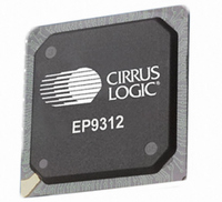
EP9312-CBZ Cirrus Logic Inc, EP9312-CBZ Datasheet - Page 777

EP9312-CBZ
Manufacturer Part Number
EP9312-CBZ
Description
IC ARM9 SOC UNIVERSAL 352PBGA
Manufacturer
Cirrus Logic Inc
Series
EP9r
Specifications of EP9312-CBZ
Core Size
16/32-Bit
Core Processor
ARM9
Speed
200MHz
Connectivity
EBI/EMI, EIDE, Ethernet, I²C, IrDA, Keypad/Touchscreen, SPI, UART/USART, USB
Peripherals
AC'97, DMA, I²:S, LCD, LED, MaverickKey, POR, PWM, WDT
Number Of I /o
16
Program Memory Type
ROMless
Ram Size
32K x 8
Voltage - Supply (vcc/vdd)
1.65 V ~ 3.6 V
Data Converters
A/D 8x12b
Oscillator Type
External
Operating Temperature
0°C ~ 70°C
Package / Case
352-BGA
Controller Family/series
(ARM9)
No. Of I/o's
16
Ram Memory Size
16MB
Cpu Speed
200MHz
No. Of Timers
4
No. Of Pwm Channels
2
Digital Ic Case Style
BGA
Embedded Interface Type
AC97, I2S, SPI, UART, USB
Rohs Compliant
Yes
Processor Series
EP93xx
Core
ARM920T
Data Bus Width
32 bit
3rd Party Development Tools
MDK-ARM, RL-ARM, ULINK2
Lead Free Status / RoHS Status
Lead free / RoHS Compliant
Eeprom Size
-
Program Memory Size
-
Lead Free Status / Rohs Status
Details
Other names
598-1258
Available stocks
Company
Part Number
Manufacturer
Quantity
Price
- Current page: 777 of 824
- Download datasheet (13Mb)
DS785UM1
27.2.7 DMA Request Latency
27.2.7.1 DMA Request Deassertion
27.2.7.2 DMA Request Latency Overview
latching of the data. It is calculated that the cycle time of AHB clock has to be smaller than
(IDE cycle time)*2/3. For different UDMA speed modes, the minimum AHB clock speeds are
listed below. There is no special speed constraint imposed on the design for PIO and MDMA
modes.
Multi-word DMA Write to IDE Controller:
The DMAide signal deassertion is generated based on the AHB write logic. The act of writing
to the Multi-word DMA write-FIFO causes the deassertion to appear on the following bus
cycle.
Multi-word DMA Read from IDE Controller:
The DMAide signal deassertion is generated based on the AHB read logic. The act of
reading from the Multi-word DMA read-FIFO causes the deassertion to appear on the
following bus cycle.
Ultra DMA Write to IDE Controller:
The DMAide signal deassertion is generated based on the contents of the Ultra DMA write
FIFO. If the FIFO contains four or more elements, the DMAide signal deasserts.
Ultra DMA Read from IDE Controller:
The DMAide signal deassertion is generated based on an internal counter. The DMAide
signal will deassert if four DMA reads have occurred or if the FIFO is now empty (which only
occurs at the end of a non-quad word aligned read from the IDE device)
The IDE controller requires a certain number of cycles to deassert the DMA request line
DMAide after a DMA access for Multi-word DMA and Ultra DMA modes. The number of wait-
states required are listed below in addition to the pipeline breakdown of the signal
propagation. The assumption is that the deassertion should follow an AHB bus command
(read or write) in HCLK cycle 1.
UDMA Speed Mode
0
1
2
3
4
Table 27-2. IDE Cycle Times and Data Transfer Rates
Min. IDE Cycle Time
Copyright 2007 Cirrus Logic
112 ns
73 ns
54 ns
39 ns
25 ns
Max. AHB Cycle
74.7 ns
48.7 ns
36.0 ns
26.0 ns
16.7 ns
Time
Min. AHB Clock
Frequency
13.4 MHz
20.5 MHz
27.8 MHz
38.5 MHz
59.8 MHz
EP93xx User’s Guide
IDE Interface
27-7
27
Related parts for EP9312-CBZ
Image
Part Number
Description
Manufacturer
Datasheet
Request
R

Part Number:
Description:
IC ARM920T MCU 200MHZ 352-PBGA
Manufacturer:
Cirrus Logic Inc
Datasheet:

Part Number:
Description:
System-on-Chip Processor
Manufacturer:
Cirrus Logic Inc
Datasheet:

Part Number:
Description:
IC ARM920T MCU 200MHZ 352-PBGA
Manufacturer:
Cirrus Logic Inc
Datasheet:

Part Number:
Description:
Development Kit
Manufacturer:
Cirrus Logic Inc
Datasheet:

Part Number:
Description:
Development Kit
Manufacturer:
Cirrus Logic Inc
Datasheet:

Part Number:
Description:
High-efficiency PFC + Fluorescent Lamp Driver Reference Design
Manufacturer:
Cirrus Logic Inc
Datasheet:

Part Number:
Description:
Development Kit
Manufacturer:
Cirrus Logic Inc
Datasheet:

Part Number:
Description:
Development Kit
Manufacturer:
Cirrus Logic Inc
Datasheet:

Part Number:
Description:
Development Kit
Manufacturer:
Cirrus Logic Inc
Datasheet:

Part Number:
Description:
Development Kit
Manufacturer:
Cirrus Logic Inc
Datasheet:

Part Number:
Description:
Development Kit
Manufacturer:
Cirrus Logic Inc
Datasheet:

Part Number:
Description:
Development Kit
Manufacturer:
Cirrus Logic Inc
Datasheet:

Part Number:
Description:
Ref Bd For Speakerbar MSA & DSP Products
Manufacturer:
Cirrus Logic Inc


