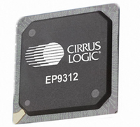
EP9312-CBZ Cirrus Logic Inc, EP9312-CBZ Datasheet - Page 235

EP9312-CBZ
Manufacturer Part Number
EP9312-CBZ
Description
IC ARM9 SOC UNIVERSAL 352PBGA
Manufacturer
Cirrus Logic Inc
Series
EP9r
Specifications of EP9312-CBZ
Core Size
16/32-Bit
Core Processor
ARM9
Speed
200MHz
Connectivity
EBI/EMI, EIDE, Ethernet, I²C, IrDA, Keypad/Touchscreen, SPI, UART/USART, USB
Peripherals
AC'97, DMA, I²:S, LCD, LED, MaverickKey, POR, PWM, WDT
Number Of I /o
16
Program Memory Type
ROMless
Ram Size
32K x 8
Voltage - Supply (vcc/vdd)
1.65 V ~ 3.6 V
Data Converters
A/D 8x12b
Oscillator Type
External
Operating Temperature
0°C ~ 70°C
Package / Case
352-BGA
Controller Family/series
(ARM9)
No. Of I/o's
16
Ram Memory Size
16MB
Cpu Speed
200MHz
No. Of Timers
4
No. Of Pwm Channels
2
Digital Ic Case Style
BGA
Embedded Interface Type
AC97, I2S, SPI, UART, USB
Rohs Compliant
Yes
Processor Series
EP93xx
Core
ARM920T
Data Bus Width
32 bit
3rd Party Development Tools
MDK-ARM, RL-ARM, ULINK2
Lead Free Status / RoHS Status
Lead free / RoHS Compliant
Eeprom Size
-
Program Memory Size
-
Lead Free Status / Rohs Status
Details
Other names
598-1258
Available stocks
Company
Part Number
Manufacturer
Quantity
Price
- Current page: 235 of 824
- Download datasheet (13Mb)
DS785UM1
CCIREN:
LCDEN:
ACEN:
INVCLK:
Copyright 2007 Cirrus Logic
V_CSYNC --> D7 (Smart Panel)
HSYNC --> D6
BLANK --> D5
P17 --> D4
P3 --> D3
P[2:0] --> D[2:0]
SPCLK --> E
A Smart Panel has an integrated controller and frame
buffer. Smart Panel R/W and RS signals must be
implemented via GPIOs and controlled via software.
CCIR Enable - Read/Write
The value written to this bit selects which video output
signals are generated:
0 - Normal signals
1 - CCIR656 YCrCb digital video signals
LCD Enable - Read/Write
The value written to this bit specifies the function of the
signals to the P[16] pin and P[15] pin:
0 - Pixel data bits 16 and 15 are routed to pins P16 and
P15, respectively
1 - XECL and YSCL signals are routed to pins P16 and
P15, respectively. The XECL and YSCL signals are used
to enable LCD drivers and register shifting
AC Enable - Read/Write
Writing ACEN = ‘1’ routes an LCD AC Waveform to pin
P17.
0 - Pixel data bit 17 is routed to pin P17
1 - LCD AC Wave Form is routed to pin P17. The
waveform toggles with each new vertical frame.
Invert Pixel Clock - Read/Write
The value written to this bit selects the active edge of
SPCLK on the SPCLK pin:
0 - Pixel data output changes on the rising edge of the
clock on the SPCLK pin
Raster Engine With Analog/LCD Integrated Timing and Interface
EP93xx User’s Guide
7-53
7
Related parts for EP9312-CBZ
Image
Part Number
Description
Manufacturer
Datasheet
Request
R

Part Number:
Description:
IC ARM920T MCU 200MHZ 352-PBGA
Manufacturer:
Cirrus Logic Inc
Datasheet:

Part Number:
Description:
System-on-Chip Processor
Manufacturer:
Cirrus Logic Inc
Datasheet:

Part Number:
Description:
IC ARM920T MCU 200MHZ 352-PBGA
Manufacturer:
Cirrus Logic Inc
Datasheet:

Part Number:
Description:
Development Kit
Manufacturer:
Cirrus Logic Inc
Datasheet:

Part Number:
Description:
Development Kit
Manufacturer:
Cirrus Logic Inc
Datasheet:

Part Number:
Description:
High-efficiency PFC + Fluorescent Lamp Driver Reference Design
Manufacturer:
Cirrus Logic Inc
Datasheet:

Part Number:
Description:
Development Kit
Manufacturer:
Cirrus Logic Inc
Datasheet:

Part Number:
Description:
Development Kit
Manufacturer:
Cirrus Logic Inc
Datasheet:

Part Number:
Description:
Development Kit
Manufacturer:
Cirrus Logic Inc
Datasheet:

Part Number:
Description:
Development Kit
Manufacturer:
Cirrus Logic Inc
Datasheet:

Part Number:
Description:
Development Kit
Manufacturer:
Cirrus Logic Inc
Datasheet:

Part Number:
Description:
Development Kit
Manufacturer:
Cirrus Logic Inc
Datasheet:

Part Number:
Description:
Ref Bd For Speakerbar MSA & DSP Products
Manufacturer:
Cirrus Logic Inc


