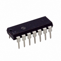
PIC16F688-I/P Microchip Technology, PIC16F688-I/P Datasheet - Page 75

PIC16F688-I/P
Manufacturer Part Number
PIC16F688-I/P
Description
IC PIC MCU FLASH 4KX14 14DIP
Manufacturer
Microchip Technology
Series
PIC® 16Fr
Datasheets
1.PIC16F616T-ISL.pdf
(8 pages)
2.PIC16F688T-ISL.pdf
(204 pages)
3.PIC16F688T-ISL.pdf
(6 pages)
4.PIC16F688T-ISL.pdf
(4 pages)
5.PIC16F688T-ISL.pdf
(688 pages)
6.PIC16F688-EP.pdf
(174 pages)
Specifications of PIC16F688-I/P
Program Memory Type
FLASH
Program Memory Size
7KB (4K x 14)
Package / Case
14-DIP (0.300", 7.62mm)
Core Processor
PIC
Core Size
8-Bit
Speed
20MHz
Connectivity
UART/USART
Peripherals
Brown-out Detect/Reset, POR, WDT
Number Of I /o
12
Eeprom Size
256 x 8
Ram Size
256 x 8
Voltage - Supply (vcc/vdd)
2 V ~ 5.5 V
Data Converters
A/D 8x10b
Oscillator Type
Internal
Operating Temperature
-40°C ~ 85°C
Processor Series
PIC16F
Core
PIC
Data Bus Width
8 bit
Data Ram Size
256 B
Interface Type
SCI/USART
Maximum Clock Frequency
20 MHz
Number Of Programmable I/os
12
Number Of Timers
2
Operating Supply Voltage
2 V to 5.5 V
Maximum Operating Temperature
+ 85 C
Mounting Style
Through Hole
3rd Party Development Tools
52715-96, 52716-328, 52717-734
Development Tools By Supplier
PG164130, DV164035, DV244005, DV164005, PG164120, ICE2000, DM163014, DM164120-4
Minimum Operating Temperature
- 40 C
On-chip Adc
8-ch x 10-bit
Data Rom Size
256 B
Height
3.3 mm
Length
19.05 mm
Supply Voltage (max)
5.5 V
Supply Voltage (min)
2 V
Width
6.35 mm
Lead Free Status / RoHS Status
Lead free / RoHS Compliant
For Use With
AC162066 - HEADER INTRFC MPLAB ICD2 20PINAC162061 - HEADER INTRFC MPLAB ICD2 20PINDM163029 - BOARD PICDEM FOR MECHATRONICSAC162056 - HEADER INTERFACE ICD2 16F688ACICE0207 - MPLABICE 14P 300 MIL ADAPTERAC124001 - MODULE SKT PROMATEII 8DIP/SOIC
Lead Free Status / Rohs Status
Lead free / RoHS Compliant
Available stocks
Company
Part Number
Manufacturer
Quantity
Price
Company:
Part Number:
PIC16F688-I/P
Manufacturer:
MICROCHIP
Quantity:
26
Company:
Part Number:
PIC16F688-I/P
Manufacturer:
MOT
Quantity:
61
9.1.2
To read a data memory location, the user must write the
address to the EEADR register, clear the EEPGD
control bit (EECON1<7>), and then set control bit RD
(EECON1<0>). The data is available in the very next
cycle, in the EEDAT register; therefore, it can be read
in the next instruction. EEDAT will hold this value until
another read or until it is written to by the user (during
a write operation).
EXAMPLE 9-1:
EXAMPLE 9-2:
2004 Microchip Technology Inc.
BSF
BCF
MOVLW
MOVWF
BCF
BSF
MOVF
BSF
BCF
MOVLW
MOVWF
MOVLW
MOVWF
BCF
BSF
BCF
MOVLW
MOVWF
MOVLW
MOVWF
BSF
BSF
SLEEP
BCF
READING THE DATA EEPROM
MEMORY
STATUS, RP0
STATUS, RP1
DATA_EE_ADDR
EEADR
EECON1, EEPGD ; Point to DATA
EECON1, RD
EEDAT, W
STATUS, RP0
STATUS, RP1
DATA_EE_ADDR
EEADR
DATA_EE_DATA
EEDAT
EECON1, EEPGD ; Point to DATA memory
EECON1, WREN
INTCON, GIE
55h
EECON2
AAh
EECON2
EECON1, WR
INTCON, GIE
EECON1, WREN
DATA EEPROM READ
DATA EEPROM WRITE
; W = EEDAT
;
; Bank 1
;
; Data Memory
; Address to read
; memory
; EE Read
; Data Memory Value to write
;
; Bank 1
;
; Data Memory Address to write
;
; Enable writes
; Disable INTs.
;
; Write 55h
;
; Write AAh
; Set WR bit to begin write
; Enable INTs.
; Wait for interrupt to signal write complete
; Disable writes
Preliminary
9.1.3
To write an EEPROM data location, the user must first
write the address to the EEADR register and the data
to the EEDAT register. Then the user must follow a
specific sequence to initiate the write for each byte.
The write will not initiate if the above sequence is not
followed exactly (write 55h to EECON2, write AAh to
EECON2, then set WR bit) for each byte. Interrupts
should be disabled during this code segment.
Additionally, the WREN bit in EECON1 must be set to
enable write. This mechanism prevents accidental
writes to data EEPROM due to errant (unexpected)
code execution (i.e., lost programs). The user should
keep the WREN bit clear at all times, except when
updating EEPROM. The WREN bit is not cleared
by hardware.
After a write sequence has been initiated, clearing the
WREN bit will not affect this write cycle. The WR bit will
be inhibited from being set unless the WREN bit is set.
At the completion of the write cycle, the WR bit is
cleared in hardware and the EE Write Complete
Interrupt Flag bit (EEIF) is set. The user can either
enable this interrupt or poll this bit. EEIF must be
cleared by software.
WRITING TO THE DATA EEPROM
MEMORY
PIC16F688
DS41203B-page 73


