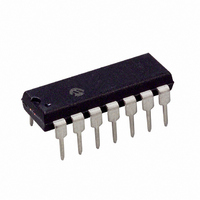
PIC16F688-I/P Microchip Technology, PIC16F688-I/P Datasheet - Page 60

PIC16F688-I/P
Manufacturer Part Number
PIC16F688-I/P
Description
IC PIC MCU FLASH 4KX14 14DIP
Manufacturer
Microchip Technology
Series
PIC® 16Fr
Datasheets
1.PIC16F616T-ISL.pdf
(8 pages)
2.PIC16F688T-ISL.pdf
(204 pages)
3.PIC16F688T-ISL.pdf
(6 pages)
4.PIC16F688T-ISL.pdf
(4 pages)
5.PIC16F688T-ISL.pdf
(688 pages)
6.PIC16F688-EP.pdf
(174 pages)
Specifications of PIC16F688-I/P
Program Memory Type
FLASH
Program Memory Size
7KB (4K x 14)
Package / Case
14-DIP (0.300", 7.62mm)
Core Processor
PIC
Core Size
8-Bit
Speed
20MHz
Connectivity
UART/USART
Peripherals
Brown-out Detect/Reset, POR, WDT
Number Of I /o
12
Eeprom Size
256 x 8
Ram Size
256 x 8
Voltage - Supply (vcc/vdd)
2 V ~ 5.5 V
Data Converters
A/D 8x10b
Oscillator Type
Internal
Operating Temperature
-40°C ~ 85°C
Processor Series
PIC16F
Core
PIC
Data Bus Width
8 bit
Data Ram Size
256 B
Interface Type
SCI/USART
Maximum Clock Frequency
20 MHz
Number Of Programmable I/os
12
Number Of Timers
2
Operating Supply Voltage
2 V to 5.5 V
Maximum Operating Temperature
+ 85 C
Mounting Style
Through Hole
3rd Party Development Tools
52715-96, 52716-328, 52717-734
Development Tools By Supplier
PG164130, DV164035, DV244005, DV164005, PG164120, ICE2000, DM163014, DM164120-4
Minimum Operating Temperature
- 40 C
On-chip Adc
8-ch x 10-bit
Data Rom Size
256 B
Height
3.3 mm
Length
19.05 mm
Supply Voltage (max)
5.5 V
Supply Voltage (min)
2 V
Width
6.35 mm
Lead Free Status / RoHS Status
Lead free / RoHS Compliant
For Use With
AC162066 - HEADER INTRFC MPLAB ICD2 20PINAC162061 - HEADER INTRFC MPLAB ICD2 20PINDM163029 - BOARD PICDEM FOR MECHATRONICSAC162056 - HEADER INTERFACE ICD2 16F688ACICE0207 - MPLABICE 14P 300 MIL ADAPTERAC124001 - MODULE SKT PROMATEII 8DIP/SOIC
Lead Free Status / Rohs Status
Lead free / RoHS Compliant
Available stocks
Company
Part Number
Manufacturer
Quantity
Price
Company:
Part Number:
PIC16F688-I/P
Manufacturer:
MICROCHIP
Quantity:
26
Company:
Part Number:
PIC16F688-I/P
Manufacturer:
MOT
Quantity:
61
PIC16F688
REGISTER 7-2:
7.4
The comparator outputs are read through the
CMCON0 register. These bits are read-only. The
comparator outputs may also be directly output to the
RA2 and RC4 I/O pins. When enabled, multiplexors in
the output path of the RA2 and RC4 pins will switch
and the output of each pin will be the unsynchronized
output of the comparator. The uncertainty of each of
the comparators is related to the input offset voltage
and the response time given in the specifications.
Figure 7-4 and Figure 7-5 show the output block
diagram for Comparator 1 and 2.
The TRIS bits will still function as an output enable/
disable for the RA2 and RC4 pins while in this mode.
The polarity of the comparator outputs can be changed
using the C1INV and C2INV bits (CMCON0<5:4>).
Timer1 gate source can be configured to use the T1G
pin or Comparator 2 output as selected by the T1GSS
bit (CMCON1<1>). This feature can be used to time the
duration or interval of analog events. The output of
Comparator 2 can also be synchronized with Timer1 by
setting the C2SYNC bit (CMCON1<0>). When
enabled, the output of Comparator 2 is latched on the
falling edge of Timer1 clock source. If a prescaler is
used with Timer1, Comparator 2 is latched after the
prescaler. To prevent a race condition, the Comparator
2 output is latched on the falling edge of the Timer1
clock source and Timer1 increments on the rising edge
of its clock source. See (Figure 7-5), Comparator 2
Block Diagram and (Figure 6-1), Timer1 Block Diagram
for more information.
It is recommended to synchronize Comparator 2 with
Timer1 by setting the C2SYNC bit when Comparator 2
is used as the Timer1 gate source. This ensures Timer1
does not miss an increment if Comparator 2 changes
during an increment.
DS41203B-page 58
Comparator Outputs
bit 7-2:
bit 1
bit 0
CMCON1 – COMPARATOR CONFIGURATION REGISTER (ADDRESS: 1Ah)
Unimplemented: Read as ‘0’
T1GSS: Timer1 Gate Source Select bit
1 = Timer1 gate source is T1G pin (RA4 must be configured as digital input)
0 = Timer1 gate source is Comparator 2 Output
C2SYNC: Comparator 2 Synchronize bit
1 = C2 output synchronized with falling edge of Timer1 clock
0 = C2 output not synchronized with Timer1 clock
bit 7
Legend:
R = Readable bit
- n = Value at POR
U-0
—
U-0
—
U-0
Preliminary
—
W = Writable bit
‘1’ = Bit is set
U-0
—
7.5
The comparator interrupt flags are set whenever there
is a change in the output value of its respective compar-
ator. Software will need to maintain information about
the status of the output bits, as read from
CMCON0<7:6>, to determine the actual change that
has occurred. The CxIF bits, PIR1<4:3>, are the
Comparator Interrupt flags. This bit must be reset in
software by clearing it to ‘0’. Since it is also possible to
write a ‘1’ to this register, a simulated interrupt may be
initiated.
The CxIE bits (PIE1<4:3>) and the PEIE bit
(INTCON<6>) must be set to enable the interrupts. In
addition, the GIE bit must also be set. If any of these
bits are cleared, the interrupt is not enabled, though the
CxIF bits will still be set if an interrupt condition occurs.
The user, in the Interrupt Service Routine, can clear the
interrupt in the following manner:
a)
b)
A mismatch condition will continue to set flag bit CxIF.
Reading CMCON0 will end the mismatch condition and
allow flag bits CxIF to be cleared.
Note:
Any read or write of CMCON0. This will end the
mismatch condition.
Clear flag bit CxIF
U = Unimplemented bit, read as ‘0’
‘0’ = Bit is cleared
Comparator Interrupts
U-0
If a change in the CMCON0 register
(CxOUT) should occur when a read
operation is being executed (start of the Q2
cycle), then the CxIF (PIR1<3>) interrupt
flag may not get set.
—
U-0
—
2004 Microchip Technology Inc.
x = Bit is unknown
T1GSS
R/W-1
C2SYNC
R/W-0
bit 0


