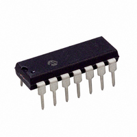
PIC16F688-I/P Microchip Technology, PIC16F688-I/P Datasheet - Page 65

PIC16F688-I/P
Manufacturer Part Number
PIC16F688-I/P
Description
IC PIC MCU FLASH 4KX14 14DIP
Manufacturer
Microchip Technology
Series
PIC® 16Fr
Datasheets
1.PIC16F616T-ISL.pdf
(8 pages)
2.PIC16F688T-ISL.pdf
(204 pages)
3.PIC16F688T-ISL.pdf
(6 pages)
4.PIC16F688T-ISL.pdf
(4 pages)
5.PIC16F688T-ISL.pdf
(688 pages)
6.PIC16F688-EP.pdf
(174 pages)
Specifications of PIC16F688-I/P
Program Memory Type
FLASH
Program Memory Size
7KB (4K x 14)
Package / Case
14-DIP (0.300", 7.62mm)
Core Processor
PIC
Core Size
8-Bit
Speed
20MHz
Connectivity
UART/USART
Peripherals
Brown-out Detect/Reset, POR, WDT
Number Of I /o
12
Eeprom Size
256 x 8
Ram Size
256 x 8
Voltage - Supply (vcc/vdd)
2 V ~ 5.5 V
Data Converters
A/D 8x10b
Oscillator Type
Internal
Operating Temperature
-40°C ~ 85°C
Processor Series
PIC16F
Core
PIC
Data Bus Width
8 bit
Data Ram Size
256 B
Interface Type
SCI/USART
Maximum Clock Frequency
20 MHz
Number Of Programmable I/os
12
Number Of Timers
2
Operating Supply Voltage
2 V to 5.5 V
Maximum Operating Temperature
+ 85 C
Mounting Style
Through Hole
3rd Party Development Tools
52715-96, 52716-328, 52717-734
Development Tools By Supplier
PG164130, DV164035, DV244005, DV164005, PG164120, ICE2000, DM163014, DM164120-4
Minimum Operating Temperature
- 40 C
On-chip Adc
8-ch x 10-bit
Data Rom Size
256 B
Height
3.3 mm
Length
19.05 mm
Supply Voltage (max)
5.5 V
Supply Voltage (min)
2 V
Width
6.35 mm
Lead Free Status / RoHS Status
Lead free / RoHS Compliant
For Use With
AC162066 - HEADER INTRFC MPLAB ICD2 20PINAC162061 - HEADER INTRFC MPLAB ICD2 20PINDM163029 - BOARD PICDEM FOR MECHATRONICSAC162056 - HEADER INTERFACE ICD2 16F688ACICE0207 - MPLABICE 14P 300 MIL ADAPTERAC124001 - MODULE SKT PROMATEII 8DIP/SOIC
Lead Free Status / Rohs Status
Lead free / RoHS Compliant
Available stocks
Company
Part Number
Manufacturer
Quantity
Price
Company:
Part Number:
PIC16F688-I/P
Manufacturer:
MICROCHIP
Quantity:
26
Company:
Part Number:
PIC16F688-I/P
Manufacturer:
MOT
Quantity:
61
8.0
The analog-to-digital converter (A/D) allows conversion
of an analog input signal to a 10-bit binary representa-
tion of that signal. The PIC16F688 has eight analog
inputs, multiplexed into one sample and hold circuit.
FIGURE 8-1:
8.1
There are three registers available to control the
functionality of the A/D module:
1.
2.
3.
8.1.1
The ANS<7:0> bits (ANSEL<7:0>) and the TRIS bits
control the operation of the A/D port pins. Set the
corresponding TRIS bits to set the pin output driver to
its
corresponding ANSEL bit to disable the digital input
buffer.
8.1.2
There are eight analog channels on the PIC16F688,
AN0
(ADCON0<4:2>) control which channel is connected to
the sample and hold circuit.
2004 Microchip Technology Inc.
Note:
ANSEL (Register 8-1)
ADCON0 (Register 8-2)
ADCON1 (Register 8-3)
high-impedance
through
ANALOG-TO-DIGITAL
CONVERTER (A/D) MODULE
A/D Configuration and Operation
ANALOG PORT PINS
Analog voltages on any pin that is defined
as a digital input may cause the input
buffer to conduct excess current.
CHANNEL SELECTION
RA1/AN1/V
AN7.
A/D BLOCK DIAGRAM
RC0/AN4
RC1/AN5
RC2/AN6
RC3/AN7
RA0/AN0
RA2/AN2
RA4/AN3
state.
REF
The
Likewise,
CHS<2:0>
CHS<2:0>
V
REF
set
Preliminary
bits
V
the
DD
GO/DONE
VCFG = 0
VCFG = 1
ADON
The output of the sample and hold is connected to the
input of the converter. The converter generates a
binary result via successive approximation and stores
the result in a 10-bit register. The voltage reference
used in the conversion is software selectable to either
V
shows the block diagram of the A/D on the PIC16F688.
8.1.3
There are two options for the voltage reference to the
A/D converter: either V
applied to V
controls the voltage reference selection. If VCFG is set,
then the voltage on the V
otherwise, V
V
DD
SS
or a voltage applied by the V
A/D
ADFM
VOLTAGE REFERENCE
REF
DD
is the reference.
is used. The VCFG bit (ADCON0<6>)
ADRESH ADRESL
DD
is used, or an analog voltage
PIC16F688
10
10
REF
pin is the reference;
REF
DS41203B-page 63
pin. Figure 8-1


