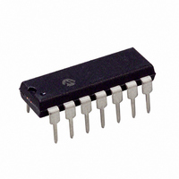
PIC16F688-I/P Microchip Technology, PIC16F688-I/P Datasheet - Page 102

PIC16F688-I/P
Manufacturer Part Number
PIC16F688-I/P
Description
IC PIC MCU FLASH 4KX14 14DIP
Manufacturer
Microchip Technology
Series
PIC® 16Fr
Datasheets
1.PIC16F616T-ISL.pdf
(8 pages)
2.PIC16F688T-ISL.pdf
(204 pages)
3.PIC16F688T-ISL.pdf
(6 pages)
4.PIC16F688T-ISL.pdf
(4 pages)
5.PIC16F688T-ISL.pdf
(688 pages)
6.PIC16F688-EP.pdf
(174 pages)
Specifications of PIC16F688-I/P
Program Memory Type
FLASH
Program Memory Size
7KB (4K x 14)
Package / Case
14-DIP (0.300", 7.62mm)
Core Processor
PIC
Core Size
8-Bit
Speed
20MHz
Connectivity
UART/USART
Peripherals
Brown-out Detect/Reset, POR, WDT
Number Of I /o
12
Eeprom Size
256 x 8
Ram Size
256 x 8
Voltage - Supply (vcc/vdd)
2 V ~ 5.5 V
Data Converters
A/D 8x10b
Oscillator Type
Internal
Operating Temperature
-40°C ~ 85°C
Processor Series
PIC16F
Core
PIC
Data Bus Width
8 bit
Data Ram Size
256 B
Interface Type
SCI/USART
Maximum Clock Frequency
20 MHz
Number Of Programmable I/os
12
Number Of Timers
2
Operating Supply Voltage
2 V to 5.5 V
Maximum Operating Temperature
+ 85 C
Mounting Style
Through Hole
3rd Party Development Tools
52715-96, 52716-328, 52717-734
Development Tools By Supplier
PG164130, DV164035, DV244005, DV164005, PG164120, ICE2000, DM163014, DM164120-4
Minimum Operating Temperature
- 40 C
On-chip Adc
8-ch x 10-bit
Data Rom Size
256 B
Height
3.3 mm
Length
19.05 mm
Supply Voltage (max)
5.5 V
Supply Voltage (min)
2 V
Width
6.35 mm
Lead Free Status / RoHS Status
Lead free / RoHS Compliant
For Use With
AC162066 - HEADER INTRFC MPLAB ICD2 20PINAC162061 - HEADER INTRFC MPLAB ICD2 20PINDM163029 - BOARD PICDEM FOR MECHATRONICSAC162056 - HEADER INTERFACE ICD2 16F688ACICE0207 - MPLABICE 14P 300 MIL ADAPTERAC124001 - MODULE SKT PROMATEII 8DIP/SOIC
Lead Free Status / Rohs Status
Lead free / RoHS Compliant
Available stocks
Company
Part Number
Manufacturer
Quantity
Price
Company:
Part Number:
PIC16F688-I/P
Manufacturer:
MICROCHIP
Quantity:
26
Company:
Part Number:
PIC16F688-I/P
Manufacturer:
MOT
Quantity:
61
PIC16F688
11.1
The configuration bits can be programmed (read as
‘0’), or left unprogrammed (read as ‘1’) to select various
device configurations as shown in Register 11-1.
These bits are mapped in program memory location
2007h.
REGISTER 11-1:
DS41203B-page 100
bit 13
bit 13-12
bit 11
bit 10
bit 9-8
bit 7
bit 6
bit 5
bit 4
bit 3
bit 2-0
—
Configuration Bits
—
Unimplemented: Read as ‘1’
FCMEN: Fail-Safe Clock Monitor Enabled bit
IESO: Internal External Switchover bit
BODEN<1:0>: Brown-out Detect Selection bits
CPD: Data Code Protection bit
CP: Code Protection bit
MCLRE: RA3/MCLR pin function select bit
PWRTE: Power-up Timer Enable bit
WDTE: Watchdog Timer Enable bit
FOSC<2:0>: Oscillator Selection bits
111 = RC oscillator: CLKOUT function on RA4/OSC2/CLKOUT pin, RC on RA5/OSC1/CLKIN
110 = RCIO oscillator: I/O function on RA4/OSC2/CLKOUT pin, RC on RA5/OSC1/CLKIN
101 = INTOSC oscillator: CLKOUT function on RA4/OSC2/CLKOUT pin, I/O function on RA5/OSC1/CLKIN
100 = INTOSCIO oscillator: I/O function on RA4/OSC2/CLKOUT pin, I/O function on RA5/OSC1/CLKIN
011 = EC: I/O function on RA4/OSC2/CLKOUT pin, CLKIN on RA5/OSC1/CLKIN
010 = HS oscillator: High-speed crystal/resonator on RA4/OSC2/CLKOUT and RA5/OSC1/CLKIN
001 = XT oscillator: Crystal/resonator on RA4/OSC2/CLKOUT and RA5/OSC1/CLKIN
000 = LP oscillator: Low-power crystal on RA4/OSC2/CLKOUT and RA5/OSC1/CLKIN
Legend:
R = Readable bit
-n = Value at POR
Note 1: Enabling Brown-out Detect does not automatically enable Power-up Timer.
FCMEN
1 = Fail-Safe Clock Monitor is enabled
0 = Fail-Safe Clock Monitor is disabled
1 = Internal External Switchover mode is enabled
0 = Internal External Switchover mode is disabled
11 = BOD enabled
10 = BOD enabled during operation and disabled in Sleep
01 = BOD controlled by SBODEN bit (PCON<4>)
00 = BOD disabled
1 = Data memory code protection is disabled
0 = Data memory code protection is enabled
1 = Program memory code protection is disabled
0 = Program memory code protection is enabled
1 = RA3/MCLR pin function is MCLR
0 = RA3/MCLR pin function is digital input, MCLR internally tied to V
1 = PWRT disabled
0 = PWRT enabled
1 = WDT enabled
0 = WDT disabled and can be enabled by SWDTEN bit (WDTCON<0>)
2: The entire data EEPROM will be erased when the code protection is turned off.
3: The entire program memory will be erased when the code protection is turned off.
4: When MCLR is asserted in INTOSC or RC mode, the internal clock oscillator is disabled.
CONFIG – CONFIGURATION WORD (ADDRESS: 2007h)
IESO
BODEN1 BODEN0
(3)
(2)
W = Writable bit
‘1’ = Bit is set
(4)
Preliminary
CPD
(1)
CP
Note:
MCLRE PWRTE WDTE
U = Unimplemented bit, read as ‘0’
‘0’ = Bit is cleared
memory space. It belongs to the special
configuration
3FFFh), which can be accessed only during
programming. See “PIC12F6XX/16F6XX
Memory
(DS41204) for more information.
Address 2007h is beyond the user program
DD
Programming
2004 Microchip Technology Inc.
memory
FOSC2 FOSC1 FOSC0
x = Bit is unknown
space
Specification”
(2000h-
bit 0


