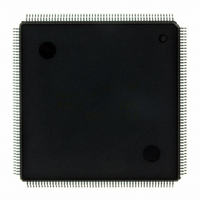
D6417709SHF200BV Renesas Electronics America, D6417709SHF200BV Datasheet - Page 39

D6417709SHF200BV
Manufacturer Part Number
D6417709SHF200BV
Description
IC SUPER H MPU ROMLESS 208LQFP
Manufacturer
Renesas Electronics America
Series
SuperH® SH7700r
Datasheet
1.D6417709SBP167BV.pdf
(809 pages)
Specifications of D6417709SHF200BV
Core Processor
SH-3
Core Size
32-Bit
Speed
200MHz
Connectivity
EBI/EMI, FIFO, IrDA, SCI, SmartCard
Peripherals
DMA, POR, WDT
Number Of I /o
96
Program Memory Type
ROMless
Ram Size
16K x 8
Voltage - Supply (vcc/vdd)
1.85 V ~ 2.15 V
Data Converters
A/D 8x10b; D/A 2x8b
Oscillator Type
Internal
Operating Temperature
-20°C ~ 75°C
Package / Case
208-QFP Exposed Pad, 208-eQFP, 208-HQFP
Lead Free Status / RoHS Status
Lead free / RoHS Compliant
Eeprom Size
-
Program Memory Size
-
Available stocks
Company
Part Number
Manufacturer
Quantity
Price
Company:
Part Number:
D6417709SHF200BV
Manufacturer:
Renesas Electronics America
Quantity:
10 000
- Current page: 39 of 809
- Download datasheet (5Mb)
Figure 23.19 Burst ROM Bus Cycle (No Wait) ........................................................................ 678
Figure 23.20 Burst ROM Bus Cycle (Two Waits) .................................................................... 679
Figure 23.21 Burst ROM Bus Cycle (External Wait, WAITSEL = 1) ...................................... 680
Figure 23.22 Synchronous DRAM Read Bus Cycle (RCD
Figure 23.23 Synchronous DRAM Read Bus Cycle (RCD
Figure 23.24 Synchronous DRAM Read Bus Cycle (Burst Read (Single Read
Figure 23.25 Synchronous DRAM Read Bus Cycle (Burst Read (Single Read
Figure 23.26 Synchronous DRAM Write Bus Cycle (RCD
Figure 23.27 Synchronous DRAM Write Bus Cycle (RCD
Figure 23.28 Synchronous DRAM Write Bus Cycle (Burst Mode (Single Write
Figure 23.29 Synchronous DRAM Write Bus Cycle (Burst Mode (Single Write
Figure 23.30 Synchronous DRAM Burst Read Bus Cycle (RAS Down, Same Row
Figure 23.31 Synchronous DRAM Burst Read Bus Cycle (RAS Down, Same Row
Figure 23.32 Synchronous DRAM Burst Read Bus Cycle (RAS Down, Different Row
Figure 23.33 Synchronous DRAM Burst Read Bus Cycle (RAS Down, Different Row
Figure 23.34 Synchronous DRAM Burst Write Bus Cycle (RAS Down, Same Row
Figure 23.35 Synchronous DRAM Burst Write Bus Cycle (RAS Down, Different Row
Figure 23.36 Synchronous DRAM Burst Write Bus Cycle (RAS Down, Different Row
Figure 23.37 Synchronous DRAM Auto-Refresh Timing (TRAS = 1, TPC = 1) ..................... 696
Figure 23.38 Synchronous DRAM Self-Refresh Cycle (TRAS
Figure 23.39 Synchronous DRAM Mode Register Write Cycle ............................................... 698
Figure 23.40 PCMCIA Memory Bus Cycle (TED = 0, TEH = 0, No Wait) ............................. 699
Figure 23.41 PCMCIA Memory Bus Cycle (TED = 2, TEH = 1, One Wait, External Wait,
Figure 23.42 PCMCIA Memory Bus Cycle (Burst Read, TED = 0, TEH = 0, No Wait).......... 701
Figure 23.43 PCMCIA Memory Bus Cycle (Burst Read, TED = 1, TEH = 1, Two Waits,
Figure 23.44 PCMCIA I/O Bus Cycle (TED = 0, TEH = 0, No Wait)...................................... 703
Figure 23.45 PCMCIA I/O Bus Cycle (TED = 2, TEH = 1, One Wait, External Wait,
Figure 23.46 PCMCIA I/O Bus Cycle (TED = 1, TEH = 1, One Wait, Bus Sizing,
RCD
RCD
RCD
RCD
Address, CAS Latency = 1).................................................................................. 689
Address, CAS Latency = 2).................................................................................. 690
Address, TPC = 0, RCD = 0, CAS Latency = 1) .................................................. 691
Address, TPC = 1, RCD = 0, CAS Latency = 1) .................................................. 692
Address) ............................................................................................................... 693
Address, TPC = 0, RCD = 0) ............................................................................... 694
Address, TPC = 1, RCD = 1) ............................................................................... 695
WAITSEL = 1)..................................................................................................... 700
Burst Pitch = 3, WAITSEL = 1)........................................................................... 702
WAITSEL = 1)..................................................................................................... 704
WAITSEL = 1)..................................................................................................... 705
0, CAS Latency
1, CAS Latency
0, TPC
1, TPC
1, TRWL = 0) ........................................................................... 687
0, TRWL = 0) ........................................................................... 688
1, TPC 1) ................................................................. 683
3, TPC 0) ................................................................. 684
0, CAS Latency
2, CAS Latency
0, TPC
2, TPC
Rev. 5.00, 09/03, page xxxvii of xliv
1, TPC
0, TRWL = 0)............ 685
1, TRWL = 1)............ 686
1) ......................... 697
1, TPC
2, TPC
4),
4),
4),
4),
0) .. 681
1) .. 682
Related parts for D6417709SHF200BV
Image
Part Number
Description
Manufacturer
Datasheet
Request
R

Part Number:
Description:
KIT STARTER FOR M16C/29
Manufacturer:
Renesas Electronics America
Datasheet:

Part Number:
Description:
KIT STARTER FOR R8C/2D
Manufacturer:
Renesas Electronics America
Datasheet:

Part Number:
Description:
R0K33062P STARTER KIT
Manufacturer:
Renesas Electronics America
Datasheet:

Part Number:
Description:
KIT STARTER FOR R8C/23 E8A
Manufacturer:
Renesas Electronics America
Datasheet:

Part Number:
Description:
KIT STARTER FOR R8C/25
Manufacturer:
Renesas Electronics America
Datasheet:

Part Number:
Description:
KIT STARTER H8S2456 SHARPE DSPLY
Manufacturer:
Renesas Electronics America
Datasheet:

Part Number:
Description:
KIT STARTER FOR R8C38C
Manufacturer:
Renesas Electronics America
Datasheet:

Part Number:
Description:
KIT STARTER FOR R8C35C
Manufacturer:
Renesas Electronics America
Datasheet:

Part Number:
Description:
KIT STARTER FOR R8CL3AC+LCD APPS
Manufacturer:
Renesas Electronics America
Datasheet:

Part Number:
Description:
KIT STARTER FOR RX610
Manufacturer:
Renesas Electronics America
Datasheet:

Part Number:
Description:
KIT STARTER FOR R32C/118
Manufacturer:
Renesas Electronics America
Datasheet:

Part Number:
Description:
KIT DEV RSK-R8C/26-29
Manufacturer:
Renesas Electronics America
Datasheet:

Part Number:
Description:
KIT STARTER FOR SH7124
Manufacturer:
Renesas Electronics America
Datasheet:

Part Number:
Description:
KIT STARTER FOR H8SX/1622
Manufacturer:
Renesas Electronics America
Datasheet:

Part Number:
Description:
KIT DEV FOR SH7203
Manufacturer:
Renesas Electronics America
Datasheet:


