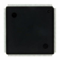
D6417709SHF200BV Renesas Electronics America, D6417709SHF200BV Datasheet - Page 272

D6417709SHF200BV
Manufacturer Part Number
D6417709SHF200BV
Description
IC SUPER H MPU ROMLESS 208LQFP
Manufacturer
Renesas Electronics America
Series
SuperH® SH7700r
Datasheet
1.D6417709SBP167BV.pdf
(809 pages)
Specifications of D6417709SHF200BV
Core Processor
SH-3
Core Size
32-Bit
Speed
200MHz
Connectivity
EBI/EMI, FIFO, IrDA, SCI, SmartCard
Peripherals
DMA, POR, WDT
Number Of I /o
96
Program Memory Type
ROMless
Ram Size
16K x 8
Voltage - Supply (vcc/vdd)
1.85 V ~ 2.15 V
Data Converters
A/D 8x10b; D/A 2x8b
Oscillator Type
Internal
Operating Temperature
-20°C ~ 75°C
Package / Case
208-QFP Exposed Pad, 208-eQFP, 208-HQFP
Lead Free Status / RoHS Status
Lead free / RoHS Compliant
Eeprom Size
-
Program Memory Size
-
Available stocks
Company
Part Number
Manufacturer
Quantity
Price
Company:
Part Number:
D6417709SHF200BV
Manufacturer:
Renesas Electronics America
Quantity:
10 000
- Current page: 272 of 809
- Download datasheet (5Mb)
Table 10.1 shows the BSC pin configuration.
Table 10.1 BSC Pins
Pin Name
Address bus
Data bus
Bus cycle start
Chip select 0, 2–4
Chip select 5, 6
PCMCIA card
select
Read/write
Row address
strobe 3L
Row address
strobe 3U
Column address
strobe
Column address
strobe LH
Data enable 0
Data enable 1
Data enable 2
Rev. 5.00, 09/03, page 226 of 760
10.1.3 Pin Configuration
Signal
A25–A0
D15–D0
D31–D16
BS
CS0, CS2–CS4
CS5/CE1A,
CS6/CE1B
CE2A, CE2B
RD/WR
RAS3L
RAS3U
CASL
CASU
WE0/DQMLL
WE1/DQMLU/
WE
WE2/DQMUL/
ICIORD
I/O
O
I/O
I/O
O
O
O
O
O
O
O
O
O
O
O
O
When memory other than synchronous DRAM is
Description
Address output
Data I/O
Data I/O when using 32-bit bus width
Shows start of bus cycle. During burst transfers,
asserted every data cycle.
Chip select signals to indicate area being accessed.
Chip select signals to indicate area being accessed.
CS5/CE1A and CS6/CE1B can also be used as
CE1A and CE1B of PCMCIA.
CE2A and CE2B signals when PCMCIA is used
Data bus direction indication signal. PCMCIA write
indication signal.
When synchronous DRAM is used, RAS3L for lower
32-Mbyte address and 64-Mbyte address.
When synchronous DRAM is used, RAS3U for
upper 32-Mbyte address.
When synchronous DRAM is used, CASL signal for
lower 32-Mbyte address and 64-Mbyte address.
When synchronous DRAM is used, CASU signal for
upper 32-Mbyte address.
used, D7–D0 write strobe signal. When
synchronous DRAM is used, selects D7–D0.
When memory other than synchronous DRAM and
PCMCIA is used, D15–D8 write strobe signal. When
synchronous DRAM is used, selects D15–D8. When
PCMCIA is used, strobe signal indicating write
cycle.
When memory other than synchronous DRAM and
PCMCIA is used, D23–D16 write strobe signal.
When synchronous DRAM is used, selects D23–
D16. When PCMCIA is used, strobe signal
indicating I/O read.
Related parts for D6417709SHF200BV
Image
Part Number
Description
Manufacturer
Datasheet
Request
R

Part Number:
Description:
KIT STARTER FOR M16C/29
Manufacturer:
Renesas Electronics America
Datasheet:

Part Number:
Description:
KIT STARTER FOR R8C/2D
Manufacturer:
Renesas Electronics America
Datasheet:

Part Number:
Description:
R0K33062P STARTER KIT
Manufacturer:
Renesas Electronics America
Datasheet:

Part Number:
Description:
KIT STARTER FOR R8C/23 E8A
Manufacturer:
Renesas Electronics America
Datasheet:

Part Number:
Description:
KIT STARTER FOR R8C/25
Manufacturer:
Renesas Electronics America
Datasheet:

Part Number:
Description:
KIT STARTER H8S2456 SHARPE DSPLY
Manufacturer:
Renesas Electronics America
Datasheet:

Part Number:
Description:
KIT STARTER FOR R8C38C
Manufacturer:
Renesas Electronics America
Datasheet:

Part Number:
Description:
KIT STARTER FOR R8C35C
Manufacturer:
Renesas Electronics America
Datasheet:

Part Number:
Description:
KIT STARTER FOR R8CL3AC+LCD APPS
Manufacturer:
Renesas Electronics America
Datasheet:

Part Number:
Description:
KIT STARTER FOR RX610
Manufacturer:
Renesas Electronics America
Datasheet:

Part Number:
Description:
KIT STARTER FOR R32C/118
Manufacturer:
Renesas Electronics America
Datasheet:

Part Number:
Description:
KIT DEV RSK-R8C/26-29
Manufacturer:
Renesas Electronics America
Datasheet:

Part Number:
Description:
KIT STARTER FOR SH7124
Manufacturer:
Renesas Electronics America
Datasheet:

Part Number:
Description:
KIT STARTER FOR H8SX/1622
Manufacturer:
Renesas Electronics America
Datasheet:

Part Number:
Description:
KIT DEV FOR SH7203
Manufacturer:
Renesas Electronics America
Datasheet:


