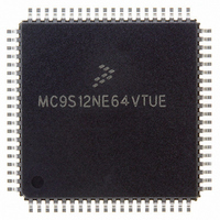
MC9S12NE64VTUE Freescale Semiconductor, MC9S12NE64VTUE Datasheet - Page 257

MC9S12NE64VTUE
Manufacturer Part Number
MC9S12NE64VTUE
Description
IC MCU 64K FLASH EEPROM 80-TQFP
Manufacturer
Freescale Semiconductor
Series
HCS12r
Datasheet
1.MC9S12NE64VTU.pdf
(554 pages)
Specifications of MC9S12NE64VTUE
Core Processor
HCS12
Core Size
16-Bit
Speed
25MHz
Connectivity
EBI/EMI, Ethernet, I²C, SCI, SPI
Peripherals
POR, PWM, WDT
Number Of I /o
38
Program Memory Size
64KB (64K x 8)
Program Memory Type
FLASH
Ram Size
8K x 8
Voltage - Supply (vcc/vdd)
2.375 V ~ 3.465 V
Data Converters
A/D 8x10b
Oscillator Type
Internal
Operating Temperature
-40°C ~ 105°C
Package / Case
80-TQFP Exposed Pad, 80-eTQFP, 80-HTQFP, 80-VQFP
Processor Series
S12N
Core
HCS12
Data Bus Width
16 bit
Data Ram Size
8 KB
Interface Type
I2C, SCI, SPI
Maximum Clock Frequency
125 MHz
Number Of Programmable I/os
70
Number Of Timers
4
Operating Supply Voltage
- 0.3 V to + 3 V
Maximum Operating Temperature
+ 105 C
Mounting Style
SMD/SMT
3rd Party Development Tools
EWHCS12
Development Tools By Supplier
EVB9S12NE64E, DEMO9S12NE64E
Minimum Operating Temperature
- 65 C
On-chip Adc
10 bit, 8 Channel
Cpu Family
HCS12
Device Core Size
16b
Frequency (max)
25MHz
Total Internal Ram Size
8KB
# I/os (max)
70
Number Of Timers - General Purpose
4
Operating Supply Voltage (typ)
2.5/3.3V
Operating Supply Voltage (max)
2.625/3.465V
Operating Supply Voltage (min)
2.357/2.375/3.135V
Instruction Set Architecture
CISC
Operating Temp Range
-40C to 105C
Operating Temperature Classification
Industrial
Mounting
Surface Mount
Pin Count
80
Package Type
TQFP
For Use With
EVB9S12NE64E - BOARD EVAL FOR 9S12NE64DEMO9S12NE64E - DEMO BOARD FOR 9S12NE64
Lead Free Status / RoHS Status
Lead free / RoHS Compliant
Eeprom Size
-
Lead Free Status / Rohs Status
Lead free / RoHS Compliant
Available stocks
Company
Part Number
Manufacturer
Quantity
Price
Company:
Part Number:
MC9S12NE64VTUE
Manufacturer:
Freescale Semiconductor
Quantity:
10 000
Part Number:
MC9S12NE64VTUE
Manufacturer:
FREESCALE
Quantity:
20 000
- Current page: 257 of 554
- Download datasheet (4Mb)
8.4.5.6.1
In this wakeup method, an idle condition on the RXD pin clears the RWU bit and wakes up the SCI. The
initial frame or frames of every message contain addressing information. All receivers evaluate the
addressing information, and receivers for which the message is addressed process the frames that follow.
Any receiver for which a message is not addressed can set its RWU bit and return to the standby state. The
RWU bit remains set and the receiver remains on standby until another idle character appears on the RXD
pin.
Idle line wakeup requires that messages be separated by at least one idle character and that no message
contains idle characters.
The idle character that wakes a receiver does not set the receiver idle bit, IDLE, or the receive data register
full flag, RDRF.
The idle line type bit, ILT, determines whether the receiver begins counting logic 1s as idle character bits
after the start bit or after the stop bit. ILT is in SCI control register 1 (SCICR1).
8.4.5.6.2
In this wakeup method, a logic 1 in the most significant bit (MSB) position of a frame clears the RWU bit
and wakes up the SCI. The logic 1 in the MSB position marks a frame as an address frame that contains
addressing information. All receivers evaluate the addressing information, and the receivers for which the
message is addressed process the frames that follow. Any receiver for which a message is not addressed
can set its RWU bit and return to the standby state. The RWU bit remains set and the receiver remains on
standby until another address frame appears on the RXD pin.
The logic 1 MSB of an address frame clears the receiver’s RWU bit before the stop bit is received and sets
the RDRF flag.
Address mark wakeup allows messages to contain idle characters but requires that the MSB be reserved
for use in address frames.
8.4.6
Normally, the SCI uses two pins for transmitting and receiving. In single-wire operation, the RXD pin is
disconnected from the SCI. The SCI uses the TXD pin for both receiving and transmitting.
Freescale Semiconductor
Single-Wire Operation
Idle Input Line Wakeup (WAKE = 0)
Address Mark Wakeup (WAKE = 1)
With the WAKE bit clear, setting the RWU bit after the RXD pin has been
idle can cause the receiver to wake up immediately.
Figure 8-24. Single-Wire Operation (LOOPS = 1, RSRC = 1)
TRANSMITTER
RECEIVER
MC9S12NE64 Data Sheet, Rev. 1.1
NOTE
RXD
TXD
Functional Description
257
Related parts for MC9S12NE64VTUE
Image
Part Number
Description
Manufacturer
Datasheet
Request
R
Part Number:
Description:
Manufacturer:
Freescale Semiconductor, Inc
Datasheet:
Part Number:
Description:
Manufacturer:
Freescale Semiconductor, Inc
Datasheet:
Part Number:
Description:
Manufacturer:
Freescale Semiconductor, Inc
Datasheet:
Part Number:
Description:
Manufacturer:
Freescale Semiconductor, Inc
Datasheet:
Part Number:
Description:
Manufacturer:
Freescale Semiconductor, Inc
Datasheet:
Part Number:
Description:
Manufacturer:
Freescale Semiconductor, Inc
Datasheet:
Part Number:
Description:
Manufacturer:
Freescale Semiconductor, Inc
Datasheet:
Part Number:
Description:
Manufacturer:
Freescale Semiconductor, Inc
Datasheet:
Part Number:
Description:
Manufacturer:
Freescale Semiconductor, Inc
Datasheet:
Part Number:
Description:
Manufacturer:
Freescale Semiconductor, Inc
Datasheet:
Part Number:
Description:
Manufacturer:
Freescale Semiconductor, Inc
Datasheet:
Part Number:
Description:
Manufacturer:
Freescale Semiconductor, Inc
Datasheet:
Part Number:
Description:
Manufacturer:
Freescale Semiconductor, Inc
Datasheet:
Part Number:
Description:
Manufacturer:
Freescale Semiconductor, Inc
Datasheet:
Part Number:
Description:
Manufacturer:
Freescale Semiconductor, Inc
Datasheet:


