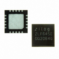
ZLF645E0Q2064G Zilog, ZLF645E0Q2064G Datasheet - Page 76

ZLF645E0Q2064G
Manufacturer Part Number
ZLF645E0Q2064G
Description
IC MCU 64K FLASH 1K RAM 20-QFN
Manufacturer
Zilog
Series
Crimzon™ ZLFr
Specifications of ZLF645E0Q2064G
Core Processor
Z8 LXMC
Core Size
8-Bit
Speed
8MHz
Connectivity
UART/USART
Peripherals
Brown-out Detect/Reset, HLVD, POR, WDT
Number Of I /o
16
Program Memory Size
64KB (64K x 8)
Program Memory Type
FLASH
Ram Size
1K x 8
Voltage - Supply (vcc/vdd)
1.9 V ~ 3.6 V
Operating Temperature
0°C ~ 70°C
Package / Case
20-VQFN Exposed Pad, 20-HVQFN, 20-SQFN, 20-DHVQFN
Lead Free Status / RoHS Status
Lead free / RoHS Compliant
Eeprom Size
-
Data Converters
-
Oscillator Type
-
Other names
269-4723
Available stocks
Company
Part Number
Manufacturer
Quantity
Price
Company:
Part Number:
ZLF645E0Q2064G
Manufacturer:
Maxim
Quantity:
28
- Current page: 76 of 197
- Download datasheet (3Mb)
PS026407-0408
Caution:
Flash Operation Timing Using Flash Frequency Registers
Flash Code Protection Against External Access
Flash Code Protection Against Accidental Program and Erasure
Before a program or erase operation on Flash memory, you must first configure the Flash
frequency High and Low Byte registers. The Flash frequency registers allow
programming and erasing of the Flash with CPU clock frequencies ranging from 1 MHz to
8 MHz. The Flash Frequency High and Low Byte registers combine to form a 16-bit value
(FFREQ) to control timing for Flash program and erase operations. The 16-bit binary
Flash Frequency value must contain two times the system clock frequency (in kHz).
This 16-bit binary Flash Frequency value is calculated using the following equation:
The System Clock Frequency depends on the Flash memory programming of bit 2 of the
User Option Byte 1 and on the register programming of bit 0 of the SMR register and can
be equal to the clock input frequency on the XTAL1 pin, a divide by 2 of that input, a divide
by 16 of that input, or a divide by 32 of that input. Flash programming and erasure are not
supported for CPU clock frequencies below 1 MHz or above 8 MHz. The Flash Frequency
High and Low Byte registers must be loaded with the correct values.
User code within the Flash main memory can be protected from external access through
the ICP or Flash Byte Programming interfaces. By use of the Flash Protect Option bits in
User Option byte 1 of the Flash Information Area, read access to the Flash’s main memory
can be blocked. For more information, see
The ZLF645 products provide several levels of protection against accidental program and
erasure of the Flash main memory contents. This protection is provided by a combination
of the register locking mechanism, the page select redundancy, and the sector level
protection control of the Flash Controller. Similar levels of protection are in place for the
Flash Information Area, minus the sector level protection.
Flash Code Protection Using Flash Controller
On Reset, the Flash Controller locks to prevent accidental program or erasure of the Flash
memory. To program or erase the Flash memory, first write the Page Select register with
the target page. Unlock the Flash Controller by making two consecutive writes to the
Flash Control register with the values
must be rewritten with the same page previously stored there. If the two Page Select writes
FREQ[15:0]
=
2x
-------------------------------------------------------------------------------------- -
System Clock Frequency (Hz)
1000
73H
Table 86
and
8CH
, sequentially. The Page Select register
on page 169.
ZLF645 Series Flash MCUs
Product Specification
Flash Controller Operation
68
Related parts for ZLF645E0Q2064G
Image
Part Number
Description
Manufacturer
Datasheet
Request
R

Part Number:
Description:
Microcontrollers (MCU) Zlf645 (32K 20L Ssop F645 (32K 20L Ssop )
Manufacturer:
Maxim Integrated Products

Part Number:
Description:
Microcontrollers (MCU) Crimzon Flash Infrared MCU
Manufacturer:
Maxim Integrated Products

Part Number:
Description:
Microcontrollers (MCU) Crimzon Flash Infrared MCU
Manufacturer:
Maxim Integrated Products

Part Number:
Description:
Microcontrollers (MCU) Crimzon Flash Infrared MCU
Manufacturer:
Maxim Integrated Products

Part Number:
Description:
Microcontrollers (MCU) Crimzon Flash Infrared MCU
Manufacturer:
Maxim Integrated Products

Part Number:
Description:
Microcontrollers (MCU) Crimzon Flash Infrared MCU
Manufacturer:
Maxim Integrated Products

Part Number:
Description:
Microcontrollers (MCU) Crimzon Flash Infrared MCU
Manufacturer:
Maxim Integrated Products

Part Number:
Description:
Microcontrollers (MCU) Crimzon Flash Infrared MCU
Manufacturer:
Maxim Integrated Products

Part Number:
Description:
Microcontrollers (MCU) Crimzon Flash Infrared MCU
Manufacturer:
Maxim Integrated Products

Part Number:
Description:
Microcontrollers (MCU) Crimzon Flash Infrared MCU
Manufacturer:
Maxim Integrated Products

Part Number:
Description:
Microcontrollers (MCU) Crimzon Flash Infrared MCU
Manufacturer:
Maxim Integrated Products

Part Number:
Description:
Microcontrollers (MCU) Crimzon Flash Infrared MCU
Manufacturer:
Maxim Integrated Products

Part Number:
Description:
Microcontrollers (MCU) Crimzon Flash Infrared MCU
Manufacturer:
Maxim Integrated Products

Part Number:
Description:
Microcontrollers (MCU) Crimzon Flash Infrared MCU
Manufacturer:
Maxim Integrated Products

Part Number:
Description:
Microcontrollers (MCU) Crimzon Flash Infrared MCU
Manufacturer:
Maxim Integrated Products


