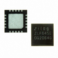
ZLF645E0Q2064G Zilog, ZLF645E0Q2064G Datasheet - Page 26

ZLF645E0Q2064G
Manufacturer Part Number
ZLF645E0Q2064G
Description
IC MCU 64K FLASH 1K RAM 20-QFN
Manufacturer
Zilog
Series
Crimzon™ ZLFr
Specifications of ZLF645E0Q2064G
Core Processor
Z8 LXMC
Core Size
8-Bit
Speed
8MHz
Connectivity
UART/USART
Peripherals
Brown-out Detect/Reset, HLVD, POR, WDT
Number Of I /o
16
Program Memory Size
64KB (64K x 8)
Program Memory Type
FLASH
Ram Size
1K x 8
Voltage - Supply (vcc/vdd)
1.9 V ~ 3.6 V
Operating Temperature
0°C ~ 70°C
Package / Case
20-VQFN Exposed Pad, 20-HVQFN, 20-SQFN, 20-DHVQFN
Lead Free Status / RoHS Status
Lead free / RoHS Compliant
Eeprom Size
-
Data Converters
-
Oscillator Type
-
Other names
269-4723
Available stocks
Company
Part Number
Manufacturer
Quantity
Price
Company:
Part Number:
ZLF645E0Q2064G
Manufacturer:
Maxim
Quantity:
28
- Current page: 26 of 197
- Download datasheet (3Mb)
I/O Port Pin Functions
PS026407-0408
RESET (Input, Active Low)
Note:
Caution:
The ZLF645 MCU features up to five 8-bit ports which are described below:
1. Port 0 is nibble-programmable as either input or output.
2. Port 1 is byte-programmable as either input or output.
3. Port 2 is bit-programmable as either input or output.
4. Port 3 features four inputs on the lower nibble and four outputs on the upper nibble.
5. Port 4 is bit-programmable as either input or output.
Port 0, Port 1, Port 2, and Port 4 internal pull-ups are disabled on any pin or group of pins
when programmed into output mode.
Reset initializes the MCU and is accomplished either through Power-On Reset (POR),
Watchdog Timer
external reset pin in the case of 48-pin packaged products.
AND P0,#%F0
The CMOS input buffer for each Port 0, Port 1, Port 2, or Port 4 pin are always
connected to the pin, even when the pin is configured as an output. If the pin is configured
as an open-drain output and no external signal is applied, a High output state can cause
the CMOS input buffer to float. This may lead to excessive leakage current of more than
100
level or ensure that its output state is Low, especially during STOP mode.
Port 0, Port 1, Port 2, and Port 4 have both input and output capability. The input logic
is always present no matter whether the port is configured as input or output. When
executing a READ instruction, the MCU reads the actual value at the input logic but not
from the
output buffer. In addition, the instructions of OR, AND, and XOR have the Read-Modify-
Write sequence. The MCU first reads the port, then modifies the value, and loads back
to the port.
Precaution must be taken, if the port is configured as an open-drain output or if the port
is driving any circuit that makes the voltage different from the appropriate output logic.
If it is configured as open-drain output with output logic as ONE, it is a floating port and
reads back as ZERO. The following instruction sets P00–P07 all Low:
μ
A. To prevent this leakage, connect the pin to an external signal with a defined logic
(WDT), Stop Mode Recovery, Low-Voltage detection, or through the
ZLF645 Series Flash MCUs
Product Specification
I/O Port Pin Functions
18
Related parts for ZLF645E0Q2064G
Image
Part Number
Description
Manufacturer
Datasheet
Request
R

Part Number:
Description:
Microcontrollers (MCU) Zlf645 (32K 20L Ssop F645 (32K 20L Ssop )
Manufacturer:
Maxim Integrated Products

Part Number:
Description:
Microcontrollers (MCU) Crimzon Flash Infrared MCU
Manufacturer:
Maxim Integrated Products

Part Number:
Description:
Microcontrollers (MCU) Crimzon Flash Infrared MCU
Manufacturer:
Maxim Integrated Products

Part Number:
Description:
Microcontrollers (MCU) Crimzon Flash Infrared MCU
Manufacturer:
Maxim Integrated Products

Part Number:
Description:
Microcontrollers (MCU) Crimzon Flash Infrared MCU
Manufacturer:
Maxim Integrated Products

Part Number:
Description:
Microcontrollers (MCU) Crimzon Flash Infrared MCU
Manufacturer:
Maxim Integrated Products

Part Number:
Description:
Microcontrollers (MCU) Crimzon Flash Infrared MCU
Manufacturer:
Maxim Integrated Products

Part Number:
Description:
Microcontrollers (MCU) Crimzon Flash Infrared MCU
Manufacturer:
Maxim Integrated Products

Part Number:
Description:
Microcontrollers (MCU) Crimzon Flash Infrared MCU
Manufacturer:
Maxim Integrated Products

Part Number:
Description:
Microcontrollers (MCU) Crimzon Flash Infrared MCU
Manufacturer:
Maxim Integrated Products

Part Number:
Description:
Microcontrollers (MCU) Crimzon Flash Infrared MCU
Manufacturer:
Maxim Integrated Products

Part Number:
Description:
Microcontrollers (MCU) Crimzon Flash Infrared MCU
Manufacturer:
Maxim Integrated Products

Part Number:
Description:
Microcontrollers (MCU) Crimzon Flash Infrared MCU
Manufacturer:
Maxim Integrated Products

Part Number:
Description:
Microcontrollers (MCU) Crimzon Flash Infrared MCU
Manufacturer:
Maxim Integrated Products

Part Number:
Description:
Microcontrollers (MCU) Crimzon Flash Infrared MCU
Manufacturer:
Maxim Integrated Products


