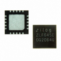
ZLF645E0Q2064G Zilog, ZLF645E0Q2064G Datasheet - Page 50

ZLF645E0Q2064G
Manufacturer Part Number
ZLF645E0Q2064G
Description
IC MCU 64K FLASH 1K RAM 20-QFN
Manufacturer
Zilog
Series
Crimzon™ ZLFr
Specifications of ZLF645E0Q2064G
Core Processor
Z8 LXMC
Core Size
8-Bit
Speed
8MHz
Connectivity
UART/USART
Peripherals
Brown-out Detect/Reset, HLVD, POR, WDT
Number Of I /o
16
Program Memory Size
64KB (64K x 8)
Program Memory Type
FLASH
Ram Size
1K x 8
Voltage - Supply (vcc/vdd)
1.9 V ~ 3.6 V
Operating Temperature
0°C ~ 70°C
Package / Case
20-VQFN Exposed Pad, 20-HVQFN, 20-SQFN, 20-DHVQFN
Lead Free Status / RoHS Status
Lead free / RoHS Compliant
Eeprom Size
-
Data Converters
-
Oscillator Type
-
Other names
269-4723
Available stocks
Company
Part Number
Manufacturer
Quantity
Price
Company:
Part Number:
ZLF645E0Q2064G
Manufacturer:
Maxim
Quantity:
28
- Current page: 50 of 197
- Download datasheet (3Mb)
PS026407-0408
Register File
Stack
The ZLF645 Series of Flash MCUs features up to 1024 bytes of register file space,
organized in 256-byte banks. Bank 0 contains 235 or 237 bytes of RAM addressed as
general purpose registers, 5 or 3 port addresses, and 16 control register addresses. For
20- or 28-pin packages, Port 1 and Port 4 registers of Bank 0 are not implemented and
there locations are available as general-purpose registers. Bank 1, Bank 2, and Bank 3;
each contain 256 general-purpose register bytes. Bank D and Bank F; each contain 16
addresses for control registers. All other banks are reserved and must not be selected.
The current bank is selected for 8-bit direct or indirect addressing by writing Register
Pointer bits RP[3:0]. In the current bank, a 16-byte working register group (addressed as
R0–R15) is selected by writing RP[7:4]. A working register operand requires only 4 bits
of Program Memory. There are 16 working register groups per bank (see
Figure
The 8-bit addresses in the range
bank-independent, meaning they always access the control registers in Bank 0, regardless
of the RP[3:0] value. Addresses in the range
registers unless Bank D or Bank F is selected (Port 01h is not implemented in this device).
When Bank D or Bank F is selected, addresses 10h–EFh access the Bank 0 general-
purpose registers.
The LDX and LDXI instructions or indirect addressing is used to access the Bank 1–3
registers not accessible by 8-bit or working register addresses (12-bit addresses—100h–
103h, 1F0h–1FFh, 200h–203h, 2F0h–2FFh, 300h–303h, and 3F0h–3FFh). See
Memory Addressing
The Stack Pointer register provides either 16-bit or 8-bit of stack pointer addressability
depending upon the programming of bit 3 of User Option Byte 1 (for more details, see
Flash Option Bits
16-bit Stack Addressability
When programmed for 16-bit stack addressability, the stack address is formed as a
combination of the SPL and SPH registers located at addresses FFh and FEh. For 1K and
512 B RAM products, the most significant 6 or 5 bits, respectively of the SPH register are
ignored. The stack address is mapped to a particular RAM memory location by the
following formula:
Bank = {2'b0, SPH[1:0]}
Group = SPL[7:4]
Register number = SPL[3:0]
With the ZLF645 MCU configured for 16-bit stack addressability, stack reads or writes to
Bank 3, 2, 1, or 0 Group F Registers or to any of the Port registers actually accesses
14).
on page 166).
on page 45.
F0h
–
FFh
(and the equivalent 4-bit addresses) are
00h
–
03h
ZLF645 Series Flash MCUs
always access the Bank 0 Port
Product Specification
Figure 13
Register File
Linear
and
42
Related parts for ZLF645E0Q2064G
Image
Part Number
Description
Manufacturer
Datasheet
Request
R

Part Number:
Description:
Microcontrollers (MCU) Zlf645 (32K 20L Ssop F645 (32K 20L Ssop )
Manufacturer:
Maxim Integrated Products

Part Number:
Description:
Microcontrollers (MCU) Crimzon Flash Infrared MCU
Manufacturer:
Maxim Integrated Products

Part Number:
Description:
Microcontrollers (MCU) Crimzon Flash Infrared MCU
Manufacturer:
Maxim Integrated Products

Part Number:
Description:
Microcontrollers (MCU) Crimzon Flash Infrared MCU
Manufacturer:
Maxim Integrated Products

Part Number:
Description:
Microcontrollers (MCU) Crimzon Flash Infrared MCU
Manufacturer:
Maxim Integrated Products

Part Number:
Description:
Microcontrollers (MCU) Crimzon Flash Infrared MCU
Manufacturer:
Maxim Integrated Products

Part Number:
Description:
Microcontrollers (MCU) Crimzon Flash Infrared MCU
Manufacturer:
Maxim Integrated Products

Part Number:
Description:
Microcontrollers (MCU) Crimzon Flash Infrared MCU
Manufacturer:
Maxim Integrated Products

Part Number:
Description:
Microcontrollers (MCU) Crimzon Flash Infrared MCU
Manufacturer:
Maxim Integrated Products

Part Number:
Description:
Microcontrollers (MCU) Crimzon Flash Infrared MCU
Manufacturer:
Maxim Integrated Products

Part Number:
Description:
Microcontrollers (MCU) Crimzon Flash Infrared MCU
Manufacturer:
Maxim Integrated Products

Part Number:
Description:
Microcontrollers (MCU) Crimzon Flash Infrared MCU
Manufacturer:
Maxim Integrated Products

Part Number:
Description:
Microcontrollers (MCU) Crimzon Flash Infrared MCU
Manufacturer:
Maxim Integrated Products

Part Number:
Description:
Microcontrollers (MCU) Crimzon Flash Infrared MCU
Manufacturer:
Maxim Integrated Products

Part Number:
Description:
Microcontrollers (MCU) Crimzon Flash Infrared MCU
Manufacturer:
Maxim Integrated Products


