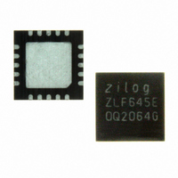
ZLF645E0Q2064G Zilog, ZLF645E0Q2064G Datasheet - Page 155

ZLF645E0Q2064G
Manufacturer Part Number
ZLF645E0Q2064G
Description
IC MCU 64K FLASH 1K RAM 20-QFN
Manufacturer
Zilog
Series
Crimzon™ ZLFr
Specifications of ZLF645E0Q2064G
Core Processor
Z8 LXMC
Core Size
8-Bit
Speed
8MHz
Connectivity
UART/USART
Peripherals
Brown-out Detect/Reset, HLVD, POR, WDT
Number Of I /o
16
Program Memory Size
64KB (64K x 8)
Program Memory Type
FLASH
Ram Size
1K x 8
Voltage - Supply (vcc/vdd)
1.9 V ~ 3.6 V
Operating Temperature
0°C ~ 70°C
Package / Case
20-VQFN Exposed Pad, 20-HVQFN, 20-SQFN, 20-DHVQFN
Lead Free Status / RoHS Status
Lead free / RoHS Compliant
Eeprom Size
-
Data Converters
-
Oscillator Type
-
Other names
269-4723
Available stocks
Company
Part Number
Manufacturer
Quantity
Price
Company:
Part Number:
ZLF645E0Q2064G
Manufacturer:
Maxim
Quantity:
28
- Current page: 155 of 197
- Download datasheet (3Mb)
Table 72. Stop Mode Recovery Register 2 (SMR2)
PS026407-0408
Bit
Field
Reset
R/W
Address
Bit Position
[7]
[6]
[5]
[4:2]
[1:0]
Note:
SMR3 Register Events
Reserved
Value
This register is not reset after a Stop Mode Recovery.
The SMR3 register can be used to configure one or more of Port 3, pins 0–3 to be
compared to a written or sampled reference value and generate a Stop Mode Recovery
event when the pin state differs from the reference value.
000
001
010
011
100
101
110
111
—
—
—
—
X
0
1
7
Description
Reserved —Read is undefined; write must be 0.
Stop Mode Recovery Level 2
Selects whether an SMR2[4:2]-selected SMR is initiated by a Low or High level at
the XOR-gate input (see
Low.
High.
Reserved —Read is undefined; Must be written to 1.
Stop Mode Recovery Source
Specifies a Stop Mode Recovery wake-up source at the XOR gate input (see
Figure 46 on page
SMR3 registers. If more than one source is selected, any selected source event
causes a Stop Mode Recovery. The following equations ignore any Port pin that
is selected in register SMR1 or configured as an output.
No SMR2 register source selected.
NAND of P23:P20.
NAND of P27:P20.
NOR of P33:P31.
NAND of P33:P31.
NOR of P33:P31, P00, P07.
NAND of P33:P31, P00, P07.
NAND of P33:P31, P22:P20.
Reserved —Read is undefined; write must be 00b.
Stop Mode Recovery
Level 2
W
6
0
146). Additional sources can be selected by SMR, SMR1, and
Bank F: 0Dh; Linear: F0Dh
Figure 46 on page
Reserved
—
X
5
W
4
Stop Mode Recovery
0
146).
Source
ZLF645 Series Flash MCUs
Reset/Stop Mode Recovery Status
W
3
0
Product Specification
W
2
0
Reserved
X
1
—
X
0
147
Related parts for ZLF645E0Q2064G
Image
Part Number
Description
Manufacturer
Datasheet
Request
R

Part Number:
Description:
Microcontrollers (MCU) Zlf645 (32K 20L Ssop F645 (32K 20L Ssop )
Manufacturer:
Maxim Integrated Products

Part Number:
Description:
Microcontrollers (MCU) Crimzon Flash Infrared MCU
Manufacturer:
Maxim Integrated Products

Part Number:
Description:
Microcontrollers (MCU) Crimzon Flash Infrared MCU
Manufacturer:
Maxim Integrated Products

Part Number:
Description:
Microcontrollers (MCU) Crimzon Flash Infrared MCU
Manufacturer:
Maxim Integrated Products

Part Number:
Description:
Microcontrollers (MCU) Crimzon Flash Infrared MCU
Manufacturer:
Maxim Integrated Products

Part Number:
Description:
Microcontrollers (MCU) Crimzon Flash Infrared MCU
Manufacturer:
Maxim Integrated Products

Part Number:
Description:
Microcontrollers (MCU) Crimzon Flash Infrared MCU
Manufacturer:
Maxim Integrated Products

Part Number:
Description:
Microcontrollers (MCU) Crimzon Flash Infrared MCU
Manufacturer:
Maxim Integrated Products

Part Number:
Description:
Microcontrollers (MCU) Crimzon Flash Infrared MCU
Manufacturer:
Maxim Integrated Products

Part Number:
Description:
Microcontrollers (MCU) Crimzon Flash Infrared MCU
Manufacturer:
Maxim Integrated Products

Part Number:
Description:
Microcontrollers (MCU) Crimzon Flash Infrared MCU
Manufacturer:
Maxim Integrated Products

Part Number:
Description:
Microcontrollers (MCU) Crimzon Flash Infrared MCU
Manufacturer:
Maxim Integrated Products

Part Number:
Description:
Microcontrollers (MCU) Crimzon Flash Infrared MCU
Manufacturer:
Maxim Integrated Products

Part Number:
Description:
Microcontrollers (MCU) Crimzon Flash Infrared MCU
Manufacturer:
Maxim Integrated Products

Part Number:
Description:
Microcontrollers (MCU) Crimzon Flash Infrared MCU
Manufacturer:
Maxim Integrated Products


