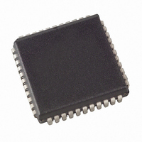
AT89C51RE2-SLSUM Atmel, AT89C51RE2-SLSUM Datasheet - Page 68

AT89C51RE2-SLSUM
Manufacturer Part Number
AT89C51RE2-SLSUM
Description
MCU 8BIT FLASH 2.7-5.5V 44-PLCC
Manufacturer
Atmel
Series
89Cr
Datasheet
1.AT89C51RE2-SLSUM.pdf
(187 pages)
Specifications of AT89C51RE2-SLSUM
Core Processor
8051
Core Size
8-Bit
Speed
60MHz
Connectivity
I²C, SPI, UART/USART
Peripherals
POR, PWM, WDT
Number Of I /o
34
Program Memory Size
128KB (128K x 8)
Program Memory Type
FLASH
Ram Size
8K x 8
Voltage - Supply (vcc/vdd)
2.7 V ~ 5.5 V
Oscillator Type
External
Operating Temperature
-40°C ~ 85°C
Package / Case
44-PLCC
Package
44PLCC
Device Core
8051
Family Name
89C
Maximum Speed
40 MHz
Operating Supply Voltage
3.3|5 V
Data Bus Width
8 Bit
Number Of Programmable I/os
34
Interface Type
SPI/TWI/UART
Number Of Timers
3
Processor Series
AT89x
Core
8051
Data Ram Size
8 KB
Maximum Clock Frequency
40 MHz
Maximum Operating Temperature
+ 85 C
Mounting Style
SMD/SMT
3rd Party Development Tools
PK51, CA51, A51, ULINK2
Development Tools By Supplier
AT89OCD-01
Minimum Operating Temperature
- 40 C
Cpu Family
89C
Device Core Size
8b
Frequency (max)
40MHz
Total Internal Ram Size
8KB
# I/os (max)
34
Number Of Timers - General Purpose
3
Operating Supply Voltage (typ)
3.3/5V
Operating Supply Voltage (max)
5.5V
Operating Supply Voltage (min)
2.7V
Instruction Set Architecture
CISC
Operating Temp Range
-40C to 85C
Operating Temperature Classification
Industrial
Mounting
Surface Mount
Pin Count
44
Package Type
PLCC
For Use With
AT89OCD-01 - USB EMULATOR FOR AT8XC51 MCUAT89STK-11 - KIT STARTER FOR AT89C51RX2
Lead Free Status / RoHS Status
Lead free / RoHS Compliant
Eeprom Size
-
Data Converters
-
Lead Free Status / Rohs Status
Lead free / RoHS Compliant
Available stocks
Company
Part Number
Manufacturer
Quantity
Price
Company:
Part Number:
AT89C51RE2-SLSUM
Manufacturer:
HONEYWELL
Quantity:
101
Timers/Counters
Timer/Counter
Operations
Timer 0
68
AT89C51RE2
The AT89C51RE2 implements two general-purpose, 16-bit Timers/Counters. Such are identified
as Timer 0 and Timer 1, and can be independently configured to operate in a variety of modes
as a Timer or an event Counter. When operating as a Timer, the Timer/Counter runs for a pro-
grammed length of time, then issues an interrupt request. When operating as a Counter, the
Timer/Counter counts negative transitions on an external pin. After a preset number of counts,
the Counter issues an interrupt request.
The various operating modes of each Timer/Counter are described in the following sections.
A basic operation is Timer registers THx and TLx (x = 0, 1) connected in cascade to form a 16-
bit Timer. Setting the run control bit (TRx) in TCON register (see Figure 46) turns the Timer on
by allowing the selected input to increment TLx. When TLx overflows it increments THx; when
THx overflows it sets the Timer overflow flag (TFx) in TCON register. Setting the TRx does not
clear the THx and TLx Timer registers. Timer registers can be accessed to obtain the current
count or to enter preset values. They can be read at any time but TRx bit must be cleared to pre-
set their values, otherwise the behavior of the Timer/Counter is unpredictable.
The C/Tx# control bit selects Timer operation or Counter operation by selecting the divided-
down peripheral clock or external pin Tx as the source for the counted signal. TRx bit must be
cleared when changing the mode of operation, otherwise the behavior of the Timer/Counter is
unpredictable.
For Timer operation (C/Tx# = 0), the Timer register counts the divided-down peripheral clock.
The Timer register is incremented once every peripheral cycle (6 peripheral clock periods). The
Timer clock rate is F
For Counter operation (C/Tx# = 1), the Timer register counts the negative transitions on the Tx
external input pin. The external input is sampled every peripheral cycles. When the sample is
high in one cycle and low in the next one, the Counter is incremented. Since it takes 2 cycles (12
peripheral clock periods) to recognize a negative transition, the maximum count rate is F
i.e. F
of the external input signal, but to ensure that a given level is sampled at least once before it
changes, it should be held for at least one full peripheral cycle.
Timer 0 functions as either a Timer or event Counter in four modes of operation. Figure 23 to
Figure 26 show the logical configuration of each mode.
Timer 0 is controlled by the four lower bits of TMOD register (see Figure 47) and bits 0, 1, 4 and
5 of TCON register (see Figure 46). TMOD register selects the method of Timer gating (GATE0),
Timer or Counter operation (T/C0#) and mode of operation (M10 and M00). TCON register pro-
vides Timer 0 control functions: overflow flag (TF0), run control bit (TR0), interrupt flag (IE0) and
interrupt type control bit (IT0).
For normal Timer operation (GATE0 = 0), setting TR0 allows TL0 to be incremented by the
selected input. Setting GATE0 and TR0 allows external pin INT0# to control Timer operation.
Timer 0 overflow (count rolls over from all 1s to all 0s) sets TF0 flag generating an interrupt
request.
It is important to stop Timer/Counter before changing mode.
OSC
/24 in standard mode or F
PER
/6, i.e. F
OSC
OSC
/12 in standard mode or F
/12 in X2 mode. There are no restrictions on the duty cycle
OSC
/6 in X2 mode.
7663E–8051–10/08
PER
/12,


