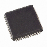
AT89C51RE2-SLSUM Atmel, AT89C51RE2-SLSUM Datasheet - Page 36

AT89C51RE2-SLSUM
Manufacturer Part Number
AT89C51RE2-SLSUM
Description
MCU 8BIT FLASH 2.7-5.5V 44-PLCC
Manufacturer
Atmel
Series
89Cr
Datasheet
1.AT89C51RE2-SLSUM.pdf
(187 pages)
Specifications of AT89C51RE2-SLSUM
Core Processor
8051
Core Size
8-Bit
Speed
60MHz
Connectivity
I²C, SPI, UART/USART
Peripherals
POR, PWM, WDT
Number Of I /o
34
Program Memory Size
128KB (128K x 8)
Program Memory Type
FLASH
Ram Size
8K x 8
Voltage - Supply (vcc/vdd)
2.7 V ~ 5.5 V
Oscillator Type
External
Operating Temperature
-40°C ~ 85°C
Package / Case
44-PLCC
Package
44PLCC
Device Core
8051
Family Name
89C
Maximum Speed
40 MHz
Operating Supply Voltage
3.3|5 V
Data Bus Width
8 Bit
Number Of Programmable I/os
34
Interface Type
SPI/TWI/UART
Number Of Timers
3
Processor Series
AT89x
Core
8051
Data Ram Size
8 KB
Maximum Clock Frequency
40 MHz
Maximum Operating Temperature
+ 85 C
Mounting Style
SMD/SMT
3rd Party Development Tools
PK51, CA51, A51, ULINK2
Development Tools By Supplier
AT89OCD-01
Minimum Operating Temperature
- 40 C
Cpu Family
89C
Device Core Size
8b
Frequency (max)
40MHz
Total Internal Ram Size
8KB
# I/os (max)
34
Number Of Timers - General Purpose
3
Operating Supply Voltage (typ)
3.3/5V
Operating Supply Voltage (max)
5.5V
Operating Supply Voltage (min)
2.7V
Instruction Set Architecture
CISC
Operating Temp Range
-40C to 85C
Operating Temperature Classification
Industrial
Mounting
Surface Mount
Pin Count
44
Package Type
PLCC
For Use With
AT89OCD-01 - USB EMULATOR FOR AT8XC51 MCUAT89STK-11 - KIT STARTER FOR AT89C51RX2
Lead Free Status / RoHS Status
Lead free / RoHS Compliant
Eeprom Size
-
Data Converters
-
Lead Free Status / Rohs Status
Lead free / RoHS Compliant
Available stocks
Company
Part Number
Manufacturer
Quantity
Price
Company:
Part Number:
AT89C51RE2-SLSUM
Manufacturer:
HONEYWELL
Quantity:
101
Access and
Operations
Descriptions
FM0 FLASH Registers
BMSEL Register
36
AT89C51RE2
The CPU interfaces to the flash memory through the FCON register, AUXR1 register and FSTA
register.
These registers are used to map the columns latch, HSB, FCB and extra row in the working data
or code space.
Table 22. BMSEL Register
BMSEL Register (S:92h)
Bank Memory Select
Reset Value= 0000 0YYYb (where YYY depends on BRV2:0 value in Fuse Configuration Byte)
Bit Number
MBO2
7-5
4-3
2-0
7
Mnemonic
MBO2:0
MBO1
FBS2:0
Bit
6
Description
Memory Bank Operation
These bits select the target memory bank for flash write or read operation. These bits
allows to read or write the on-chip flash memory from one upper 32K bytes to another
one.
0 X X: The on-chip flash operation target banked is the same as FBS2:0
1 0 0: The target memory bank is forced to Bank0
1 0 1: The target memory bank is forced to Bank1
1 1 0: The target memory bank is forced to Bank2
1 1 1: The target memory bank is forced to Bank3 (optional External bank)
Reserved
Fetch Bank Selection
These bits select the upper 32K bytes execution bank:
FBS1:0 can be read/write by software.
FBS2 is read-only by software (the Boot bank can not be mapped from FM0)
0 0 0 Bank0
0 0 1 Bank1
0 1 0 Bank2
0 1 1 Bank3 (optionnal external bank)
1 X X Boot Bank (Read only)
Upon reset FBS2:0 is initialized according to BRV2:0 configuration bits in FCB.
MBO0
5
4
3
FBS2
2
FBS1
1
7663E–8051–10/08
FBS0
0


