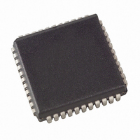
AT89C51RE2-SLSUM Atmel, AT89C51RE2-SLSUM Datasheet - Page 34

AT89C51RE2-SLSUM
Manufacturer Part Number
AT89C51RE2-SLSUM
Description
MCU 8BIT FLASH 2.7-5.5V 44-PLCC
Manufacturer
Atmel
Series
89Cr
Datasheet
1.AT89C51RE2-SLSUM.pdf
(187 pages)
Specifications of AT89C51RE2-SLSUM
Core Processor
8051
Core Size
8-Bit
Speed
60MHz
Connectivity
I²C, SPI, UART/USART
Peripherals
POR, PWM, WDT
Number Of I /o
34
Program Memory Size
128KB (128K x 8)
Program Memory Type
FLASH
Ram Size
8K x 8
Voltage - Supply (vcc/vdd)
2.7 V ~ 5.5 V
Oscillator Type
External
Operating Temperature
-40°C ~ 85°C
Package / Case
44-PLCC
Package
44PLCC
Device Core
8051
Family Name
89C
Maximum Speed
40 MHz
Operating Supply Voltage
3.3|5 V
Data Bus Width
8 Bit
Number Of Programmable I/os
34
Interface Type
SPI/TWI/UART
Number Of Timers
3
Processor Series
AT89x
Core
8051
Data Ram Size
8 KB
Maximum Clock Frequency
40 MHz
Maximum Operating Temperature
+ 85 C
Mounting Style
SMD/SMT
3rd Party Development Tools
PK51, CA51, A51, ULINK2
Development Tools By Supplier
AT89OCD-01
Minimum Operating Temperature
- 40 C
Cpu Family
89C
Device Core Size
8b
Frequency (max)
40MHz
Total Internal Ram Size
8KB
# I/os (max)
34
Number Of Timers - General Purpose
3
Operating Supply Voltage (typ)
3.3/5V
Operating Supply Voltage (max)
5.5V
Operating Supply Voltage (min)
2.7V
Instruction Set Architecture
CISC
Operating Temp Range
-40C to 85C
Operating Temperature Classification
Industrial
Mounting
Surface Mount
Pin Count
44
Package Type
PLCC
For Use With
AT89OCD-01 - USB EMULATOR FOR AT8XC51 MCUAT89STK-11 - KIT STARTER FOR AT89C51RX2
Lead Free Status / RoHS Status
Lead free / RoHS Compliant
Eeprom Size
-
Data Converters
-
Lead Free Status / Rohs Status
Lead free / RoHS Compliant
Available stocks
Company
Part Number
Manufacturer
Quantity
Price
Company:
Part Number:
AT89C51RE2-SLSUM
Manufacturer:
HONEYWELL
Quantity:
101
Fuse Configuration Byte
(FCB)
34
AT89C51RE2
The Fuse configuration byte is a part of FM0.
The 8 bits read/written by software (from FM0 or RM0) and written by hardware in parallel mode.
Table 20. Fuse Configuration Byte (FCB)
Number
Bit
6-3
2-0
X2
7
7
Mnemonic
BRV2-0-
Bit
X2
-
6
-
Description
X2 Mode
Unused
Boot Reset Vector
These bits allow to configure the reset vector of the product according to the following
values:
1 1 1: Reset at address 0x0000 of FM0 with Bank0 mapped
1 1 0: Reset at address 0xFFFC of Bank 0
1 0 1: Reset at address 0xFFFC of Bank 1
1 0 0: Reset at address 0xFFFC of Bank 2
0 1 1: Reset at address 0x0000 of RM0 (Internal ROM bootloader execution)
0 1 0: Reserved for further extension but same as 1 1 1
0 0 1: Reserved for further extension but same as 1 1 1
0 0 0: Reserved for further extension but same as 1 1 1
5
Programmed (‘0’ value) to force X2 mode (6 clocks per instruction) after reset
Unprogrammed (‘1’ value) to force X1 mode, Standard Mode, after reset (Default)
-
4
-
3
-
BRV2
2
BRV1
1
7663E–8051–10/08
BRV0
0


