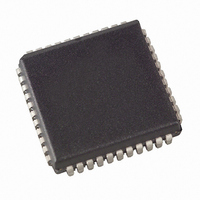
AT89C51RE2-SLSUM Atmel, AT89C51RE2-SLSUM Datasheet - Page 43

AT89C51RE2-SLSUM
Manufacturer Part Number
AT89C51RE2-SLSUM
Description
MCU 8BIT FLASH 2.7-5.5V 44-PLCC
Manufacturer
Atmel
Series
89Cr
Datasheet
1.AT89C51RE2-SLSUM.pdf
(187 pages)
Specifications of AT89C51RE2-SLSUM
Core Processor
8051
Core Size
8-Bit
Speed
60MHz
Connectivity
I²C, SPI, UART/USART
Peripherals
POR, PWM, WDT
Number Of I /o
34
Program Memory Size
128KB (128K x 8)
Program Memory Type
FLASH
Ram Size
8K x 8
Voltage - Supply (vcc/vdd)
2.7 V ~ 5.5 V
Oscillator Type
External
Operating Temperature
-40°C ~ 85°C
Package / Case
44-PLCC
Package
44PLCC
Device Core
8051
Family Name
89C
Maximum Speed
40 MHz
Operating Supply Voltage
3.3|5 V
Data Bus Width
8 Bit
Number Of Programmable I/os
34
Interface Type
SPI/TWI/UART
Number Of Timers
3
Processor Series
AT89x
Core
8051
Data Ram Size
8 KB
Maximum Clock Frequency
40 MHz
Maximum Operating Temperature
+ 85 C
Mounting Style
SMD/SMT
3rd Party Development Tools
PK51, CA51, A51, ULINK2
Development Tools By Supplier
AT89OCD-01
Minimum Operating Temperature
- 40 C
Cpu Family
89C
Device Core Size
8b
Frequency (max)
40MHz
Total Internal Ram Size
8KB
# I/os (max)
34
Number Of Timers - General Purpose
3
Operating Supply Voltage (typ)
3.3/5V
Operating Supply Voltage (max)
5.5V
Operating Supply Voltage (min)
2.7V
Instruction Set Architecture
CISC
Operating Temp Range
-40C to 85C
Operating Temperature Classification
Industrial
Mounting
Surface Mount
Pin Count
44
Package Type
PLCC
For Use With
AT89OCD-01 - USB EMULATOR FOR AT8XC51 MCUAT89STK-11 - KIT STARTER FOR AT89C51RX2
Lead Free Status / RoHS Status
Lead free / RoHS Compliant
Eeprom Size
-
Data Converters
-
Lead Free Status / Rohs Status
Lead free / RoHS Compliant
Available stocks
Company
Part Number
Manufacturer
Quantity
Price
Company:
Part Number:
AT89C51RE2-SLSUM
Manufacturer:
HONEYWELL
Quantity:
101
Extra Row
Hardware Security Byte
(HSB)
7663E–8051–10/08
The following procedure is used to program the Extra Row space and is summarized in
Figure 14:
•
•
•
•
Figure 14. Flash and Extra row Programming Procedure
The following procedure is used to program the Hardware
summarized in Figure 15:
•
•
•
•
•
Load data in the column latches from address FF80h to FFFFh.
Disable the interrupts.
Launch the programming by writing the data sequence 51h followed by A1h in FCON
register.
The end of the programming indicated by the FBUSY flag cleared.
Enable the interrupts.
Set FPS and map Hardware byte (FCON = 0x0C)
Save and disable the interrupts.
Load DPTR at address 0000h
Load Accumulator register with the data to load.
Execute the MOVX @DPTR, A instruction.
Column Latches Loading
Launch Programming
End Programming
Save & Disable IT
Programming
see Figure 13
FCON = 00h
FCON= A0h
FCON= 50h
Clear Mode
Cleared?
Restore IT
FBusy
Flash
EA= 0
Column Latches Loading
Launch Programming
End Programming
Save & Disable IT
Programming
see Figure 13
FCON = 00h
Security
FCON= 51h
FCON= A1h
Clear Mode
Cleared?
Restore IT
XROW
FBusy
EA= 0
AT89C51RE2
Byte space and is
43


