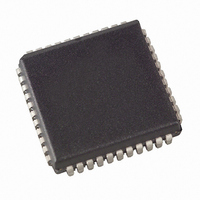
AT89C51RE2-SLSUM Atmel, AT89C51RE2-SLSUM Datasheet - Page 47

AT89C51RE2-SLSUM
Manufacturer Part Number
AT89C51RE2-SLSUM
Description
MCU 8BIT FLASH 2.7-5.5V 44-PLCC
Manufacturer
Atmel
Series
89Cr
Datasheet
1.AT89C51RE2-SLSUM.pdf
(187 pages)
Specifications of AT89C51RE2-SLSUM
Core Processor
8051
Core Size
8-Bit
Speed
60MHz
Connectivity
I²C, SPI, UART/USART
Peripherals
POR, PWM, WDT
Number Of I /o
34
Program Memory Size
128KB (128K x 8)
Program Memory Type
FLASH
Ram Size
8K x 8
Voltage - Supply (vcc/vdd)
2.7 V ~ 5.5 V
Oscillator Type
External
Operating Temperature
-40°C ~ 85°C
Package / Case
44-PLCC
Package
44PLCC
Device Core
8051
Family Name
89C
Maximum Speed
40 MHz
Operating Supply Voltage
3.3|5 V
Data Bus Width
8 Bit
Number Of Programmable I/os
34
Interface Type
SPI/TWI/UART
Number Of Timers
3
Processor Series
AT89x
Core
8051
Data Ram Size
8 KB
Maximum Clock Frequency
40 MHz
Maximum Operating Temperature
+ 85 C
Mounting Style
SMD/SMT
3rd Party Development Tools
PK51, CA51, A51, ULINK2
Development Tools By Supplier
AT89OCD-01
Minimum Operating Temperature
- 40 C
Cpu Family
89C
Device Core Size
8b
Frequency (max)
40MHz
Total Internal Ram Size
8KB
# I/os (max)
34
Number Of Timers - General Purpose
3
Operating Supply Voltage (typ)
3.3/5V
Operating Supply Voltage (max)
5.5V
Operating Supply Voltage (min)
2.7V
Instruction Set Architecture
CISC
Operating Temp Range
-40C to 85C
Operating Temperature Classification
Industrial
Mounting
Surface Mount
Pin Count
44
Package Type
PLCC
For Use With
AT89OCD-01 - USB EMULATOR FOR AT8XC51 MCUAT89STK-11 - KIT STARTER FOR AT89C51RX2
Lead Free Status / RoHS Status
Lead free / RoHS Compliant
Eeprom Size
-
Data Converters
-
Lead Free Status / Rohs Status
Lead free / RoHS Compliant
Available stocks
Company
Part Number
Manufacturer
Quantity
Price
Company:
Part Number:
AT89C51RE2-SLSUM
Manufacturer:
HONEYWELL
Quantity:
101
Errors Report /
Miscellaneous states
Flash Busy flag
Flash Programming
Sequence Error
Power Down Mode
Request
7663E–8051–10/08
The FBUSY flag indicates on-going flash write operation.
The busy flag is set by hardware, the hardware clears this flag after the end of the programming
operation.
When a wrong sequence is detected the FSE in FSTA is set.
The following events are considered as not correct activation sequence:
- The two “MOV FCON,5x and MOV FCON, Ax” were not consecutive, or the second instruction
differs from “MOV FCON Ax” (for example, an interrupt occurs during the sequence).
- The sequence (write flash or reset column latches) occurred with no data loaded in the column
latches
The FSE bit can be cleared:
- By software
- By hardware when a correct programming sequence occurs.
Note: When a good sequence occurs just after an incorrect sequence, the previous error is lost.
The user software application should take care to check the FSE bit before initiating a new
sequence.
In Power Down mode, the on-chip flash memory is deselected (to reduce power consumption),
this leads to the lost of the columns latches content.
In this case, if columns latches were previously loaded they are reset: FLOAD bit in FSTA regis-
ter should be reset after power down mode.
If a power down mode is requested during flash programming (FBUSY=1), all power down
sequence instructions should be ignored until the end of flash process.
AT89C51RE2
47


