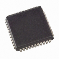
AT89C51RE2-SLSUM Atmel, AT89C51RE2-SLSUM Datasheet - Page 174

AT89C51RE2-SLSUM
Manufacturer Part Number
AT89C51RE2-SLSUM
Description
MCU 8BIT FLASH 2.7-5.5V 44-PLCC
Manufacturer
Atmel
Series
89Cr
Datasheet
1.AT89C51RE2-SLSUM.pdf
(187 pages)
Specifications of AT89C51RE2-SLSUM
Core Processor
8051
Core Size
8-Bit
Speed
60MHz
Connectivity
I²C, SPI, UART/USART
Peripherals
POR, PWM, WDT
Number Of I /o
34
Program Memory Size
128KB (128K x 8)
Program Memory Type
FLASH
Ram Size
8K x 8
Voltage - Supply (vcc/vdd)
2.7 V ~ 5.5 V
Oscillator Type
External
Operating Temperature
-40°C ~ 85°C
Package / Case
44-PLCC
Package
44PLCC
Device Core
8051
Family Name
89C
Maximum Speed
40 MHz
Operating Supply Voltage
3.3|5 V
Data Bus Width
8 Bit
Number Of Programmable I/os
34
Interface Type
SPI/TWI/UART
Number Of Timers
3
Processor Series
AT89x
Core
8051
Data Ram Size
8 KB
Maximum Clock Frequency
40 MHz
Maximum Operating Temperature
+ 85 C
Mounting Style
SMD/SMT
3rd Party Development Tools
PK51, CA51, A51, ULINK2
Development Tools By Supplier
AT89OCD-01
Minimum Operating Temperature
- 40 C
Cpu Family
89C
Device Core Size
8b
Frequency (max)
40MHz
Total Internal Ram Size
8KB
# I/os (max)
34
Number Of Timers - General Purpose
3
Operating Supply Voltage (typ)
3.3/5V
Operating Supply Voltage (max)
5.5V
Operating Supply Voltage (min)
2.7V
Instruction Set Architecture
CISC
Operating Temp Range
-40C to 85C
Operating Temperature Classification
Industrial
Mounting
Surface Mount
Pin Count
44
Package Type
PLCC
For Use With
AT89OCD-01 - USB EMULATOR FOR AT8XC51 MCUAT89STK-11 - KIT STARTER FOR AT89C51RX2
Lead Free Status / RoHS Status
Lead free / RoHS Compliant
Eeprom Size
-
Data Converters
-
Lead Free Status / Rohs Status
Lead free / RoHS Compliant
Available stocks
Company
Part Number
Manufacturer
Quantity
Price
Company:
Part Number:
AT89C51RE2-SLSUM
Manufacturer:
HONEYWELL
Quantity:
101
External Data Memory Read Cycle
Serial Port Timing -
Shift Register Mode
174
AT89C51RE2
PORT 0
PORT 2
ALE
PSEN
RD
OR SFR-P2
ADDRESS
Table 125. Symbol Description
Table 126. AC Parameters for a Fix Clock
Notes:
Symbol
T
T
T
T
T
Symbol
QVHX
XHQX
XHDX
XHDV
XLXL
1. ‘ -L ‘ refers to 2V - 5.5V version.
2. ‘ -M ’ refers to 4.5V to 5.5V version.
T
T
T
T
T
QVHX
XHQX
XHDX
XHDV
XLXL
A0-A7
T
Parameter
Serial port clock cycle time
Output data set-up to clock rising edge
Output data hold after clock rising edge
Input data hold after clock rising edge
Clock rising edge to input data valid
Min
LLAX
T
300
200
30
AVWL
0
T
LLWL
T
-M
AVDV
T
(1)
LLDV
ADDRESS A8-A15 OR SFR P2
Max
117
T
RLAZ
T
RLRH
Min
300
200
30
0
DATA IN
-L
T
(2)
T
WHLH
RHDX
Max
117
T
RHDZ
7663E–8051–10/08
Units
ns
ns
ns
ns
ns


