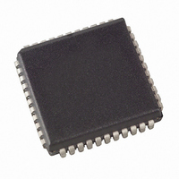
AT89C51RE2-SLSUM Atmel, AT89C51RE2-SLSUM Datasheet - Page 126

AT89C51RE2-SLSUM
Manufacturer Part Number
AT89C51RE2-SLSUM
Description
MCU 8BIT FLASH 2.7-5.5V 44-PLCC
Manufacturer
Atmel
Series
89Cr
Datasheet
1.AT89C51RE2-SLSUM.pdf
(187 pages)
Specifications of AT89C51RE2-SLSUM
Core Processor
8051
Core Size
8-Bit
Speed
60MHz
Connectivity
I²C, SPI, UART/USART
Peripherals
POR, PWM, WDT
Number Of I /o
34
Program Memory Size
128KB (128K x 8)
Program Memory Type
FLASH
Ram Size
8K x 8
Voltage - Supply (vcc/vdd)
2.7 V ~ 5.5 V
Oscillator Type
External
Operating Temperature
-40°C ~ 85°C
Package / Case
44-PLCC
Package
44PLCC
Device Core
8051
Family Name
89C
Maximum Speed
40 MHz
Operating Supply Voltage
3.3|5 V
Data Bus Width
8 Bit
Number Of Programmable I/os
34
Interface Type
SPI/TWI/UART
Number Of Timers
3
Processor Series
AT89x
Core
8051
Data Ram Size
8 KB
Maximum Clock Frequency
40 MHz
Maximum Operating Temperature
+ 85 C
Mounting Style
SMD/SMT
3rd Party Development Tools
PK51, CA51, A51, ULINK2
Development Tools By Supplier
AT89OCD-01
Minimum Operating Temperature
- 40 C
Cpu Family
89C
Device Core Size
8b
Frequency (max)
40MHz
Total Internal Ram Size
8KB
# I/os (max)
34
Number Of Timers - General Purpose
3
Operating Supply Voltage (typ)
3.3/5V
Operating Supply Voltage (max)
5.5V
Operating Supply Voltage (min)
2.7V
Instruction Set Architecture
CISC
Operating Temp Range
-40C to 85C
Operating Temperature Classification
Industrial
Mounting
Surface Mount
Pin Count
44
Package Type
PLCC
For Use With
AT89OCD-01 - USB EMULATOR FOR AT8XC51 MCUAT89STK-11 - KIT STARTER FOR AT89C51RX2
Lead Free Status / RoHS Status
Lead free / RoHS Compliant
Eeprom Size
-
Data Converters
-
Lead Free Status / Rohs Status
Lead free / RoHS Compliant
Available stocks
Company
Part Number
Manufacturer
Quantity
Price
Company:
Part Number:
AT89C51RE2-SLSUM
Manufacturer:
HONEYWELL
Quantity:
101
Reduced EMI
Mode
126
AT89C51RE2
The ALE signal is used to demultiplex address and data buses on port 0 when used with exter-
nal program or data memory. Nevertheless, during internal code execution, ALE signal is still
generated. In order to reduce EMI, ALE signal can be disabled by setting AO bit.
The AO bit is located in AUXR register at bit location 0. As soon as AO is set, ALE is no longer
output but remains active during MOVX and MOVC instructions and external fetches. During
ALE disabling, ALE pin is weakly pulled high.
Table 94. AUXR Register
AUXR - Auxiliary Register (8Eh)
Reset Value = XX00 10’HSB. XRAM’0b
Not bit addressable
Number
Bit
7
-
7
6
5
4
3
2
1
0
Mnemonic
EXTRAM
XRS2
XRS1
XRS0
Bit
M0
AO
6
-
-
-
Description
Reserved
The value read from this bit is indeterminate. Do not set this bit.
Reserved
The value read from this bit is indeterminate. Do not set this bit.
Pulse length
Cleared to stretch MOVX control: the RD/ and the WR/ pulse length is 6 clock periods
(default).
Set to stretch MOVX control: the RD/ and the WR/ pulse length is 30 clock periods.
XRAM Size
XRS2
0
0
0
0
1
EXTRAM bit
Cleared to access internal XRAM using movx @ Ri/ @ DPTR.
Set to access external memory.
Programmed by hardware after Power-up regarding Hardware Security Byte (HSB),
default setting, XRAM selected.
ALE Output bit
Cleared, ALE is emitted at a constant rate of 1/6 the oscillator frequency (or 1/3 if X2
mode is used). (default) Set, ALE is active only during a MOVX or MOVC instruction is
used.
M0
5
XRS1
0
0
1
1
0
XRS2
XRS0 XRAM size
0
1
0
0
1
4
256 bytes
768 bytes(default)
1024 bytes
1792 bytes
512 bytes
XRS1
3
XRS0
2
EXTRAM
1
7663E–8051–10/08
AO
0


