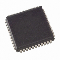
AT89C51RE2-SLSUM Atmel, AT89C51RE2-SLSUM Datasheet - Page 41

AT89C51RE2-SLSUM
Manufacturer Part Number
AT89C51RE2-SLSUM
Description
MCU 8BIT FLASH 2.7-5.5V 44-PLCC
Manufacturer
Atmel
Series
89Cr
Datasheet
1.AT89C51RE2-SLSUM.pdf
(187 pages)
Specifications of AT89C51RE2-SLSUM
Core Processor
8051
Core Size
8-Bit
Speed
60MHz
Connectivity
I²C, SPI, UART/USART
Peripherals
POR, PWM, WDT
Number Of I /o
34
Program Memory Size
128KB (128K x 8)
Program Memory Type
FLASH
Ram Size
8K x 8
Voltage - Supply (vcc/vdd)
2.7 V ~ 5.5 V
Oscillator Type
External
Operating Temperature
-40°C ~ 85°C
Package / Case
44-PLCC
Package
44PLCC
Device Core
8051
Family Name
89C
Maximum Speed
40 MHz
Operating Supply Voltage
3.3|5 V
Data Bus Width
8 Bit
Number Of Programmable I/os
34
Interface Type
SPI/TWI/UART
Number Of Timers
3
Processor Series
AT89x
Core
8051
Data Ram Size
8 KB
Maximum Clock Frequency
40 MHz
Maximum Operating Temperature
+ 85 C
Mounting Style
SMD/SMT
3rd Party Development Tools
PK51, CA51, A51, ULINK2
Development Tools By Supplier
AT89OCD-01
Minimum Operating Temperature
- 40 C
Cpu Family
89C
Device Core Size
8b
Frequency (max)
40MHz
Total Internal Ram Size
8KB
# I/os (max)
34
Number Of Timers - General Purpose
3
Operating Supply Voltage (typ)
3.3/5V
Operating Supply Voltage (max)
5.5V
Operating Supply Voltage (min)
2.7V
Instruction Set Architecture
CISC
Operating Temp Range
-40C to 85C
Operating Temperature Classification
Industrial
Mounting
Surface Mount
Pin Count
44
Package Type
PLCC
For Use With
AT89OCD-01 - USB EMULATOR FOR AT8XC51 MCUAT89STK-11 - KIT STARTER FOR AT89C51RX2
Lead Free Status / RoHS Status
Lead free / RoHS Compliant
Eeprom Size
-
Data Converters
-
Lead Free Status / Rohs Status
Lead free / RoHS Compliant
Available stocks
Company
Part Number
Manufacturer
Quantity
Price
Company:
Part Number:
AT89C51RE2-SLSUM
Manufacturer:
HONEYWELL
Quantity:
101
Loading the Column
Latches
7663E–8051–10/08
Any number of data from 0 byte to 128 bytes can be loaded in the column latches. The data writ-
ten in the column latches can be written in a none consecutive order. The DPTR allows to select
the address of the byte to load in the column latches.
The page address to be written (target page in FM0) is given by the last address loaded in the
column latches and when this page belongs to the upper 32K bytes of the logical addressable
MCU space, the target memory bank selection is performed upon the MBO2:0 value during the
last address loaded.
When 0 byte is loaded in the column latches the activation sequence (5xh, Axh in FCON) does
not launch any operations. The FSE bit in FSTA register is set.
When a current flash write operation is on-going (FBUSY is set), it is impossible to load the col-
umns latches before the end of flash programming process (the write operation in the columns
latches is not performed, and the previous columns latches content is not overwritten).
When programming is launched, an automatic erase of the entire memory page is first per-
formed, then programming is effectively done. Thus no page or block erase is needed and only
the loaded data are programmed in the corresponding page. The unloaded data of the target
memory page are programmed at 0xFF value (automatic page erase value).
The following procedure is used to load the column latches and is summarized in Figure 13:
•
•
•
•
•
•
•
•
•
Disable interrupt and map the column latch space by setting FPS bit.
Select the target memory bank (for page address larger than 32K)
Map the column latch
Reset the column latch
Load the DPTR with the address to write.
Load Accumulator register with the data to write.
Execute the MOVX @DPTR, A instruction, and only this one (no MOVX @Ri, A).
If needed loop the last three instructions until the page is completely loaded.
Unmap the column latch if needed (it can be left mapped) and Enable Interrupt
AT89C51RE2
41


