C8051F320DK Silicon Laboratories Inc, C8051F320DK Datasheet - Page 55
C8051F320DK
Manufacturer Part Number
C8051F320DK
Description
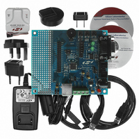
DEV KIT FOR C8051F320/F321
Manufacturer
Silicon Laboratories Inc
Type
MCUr
Specifications of C8051F320DK
Contents
Evaluation Board, Power Supply, USB Cables, Adapter and Documentation
Processor To Be Evaluated
C8051F320/F321
Interface Type
USB
Silicon Manufacturer
Silicon Labs
Core Architecture
8051
Silicon Core Number
C8051F320
Silicon Family Name
C8051F32x
Lead Free Status / RoHS Status
Contains lead / RoHS non-compliant
For Use With/related Products
Silicon Laboratories C8051F320, C8051F321
Lead Free Status / Rohs Status
Lead free / RoHS Compliant
Other names
336-1260
Available stocks
Company
Part Number
Manufacturer
Quantity
Price
Company:

Part Number:
C8051F320DK
Manufacturer:
SiliconL
Quantity:
4


6.
The Voltage reference MUX on C8051F320/1 devices is configurable to use an externally connected volt-
age reference, the internal reference voltage generator, or the power supply voltage VDD (see Figure 6.1).
The REFSL bit in the Reference Control register (REF0CN) selects the reference source. For the internal
reference or an external source, REFSL should be set to ‘0’; For VDD as the reference source, REFSL
should be set to ‘1’.
The BIASE bit enables the internal ADC bias generator, which is used by the ADC and Internal Oscillator.
This enable is forced to logic 1 when either of the aforementioned peripherals is enabled. The ADC bias
generator may be enabled manually by writing a ‘1’ to the BIASE bit in register REF0CN; see Figure 6.1 for
REF0CN register details. The Reference bias generator (see Figure 6.1) is used by the Internal Voltage
Reference, Temperature Sensor, and Clock Multiplier. The Reference bias is automatically enabled when
any of the aforementioned peripherals are enabled. The electrical specifications for the voltage reference
and bias circuits are given in Table 6.1.
Important Note About the VREF Input: Port pin P0.7 is used as the external VREF input. When using an
external voltage reference, P0.7 should be configured as analog input and skipped by the Digital Crossbar.
To configure P0.7 as analog input, set to ‘0’ Bit7 in register P0MDIN. To configure the Crossbar to skip
P0.7, set to ‘1’ Bit7 in register P0SKIP. Refer to Section “14. Port Input/Output” on page 126 for complete
Port I/O configuration details.
The temperature sensor connects to the ADC0 positive input multiplexer (see Section “5.1. Analog Multi-
plexer” on page 40 for details). The TEMPE bit in register REF0CN enables/disables the temperature sen-
sor. While disabled, the temperature sensor defaults to a high impedance state and any ADC0
measurements performed on the sensor result in meaningless data.
Voltage Reference
GND
VDD
R1
Reference
Figure 6.1. Voltage Reference Functional Block Diagram
External
Voltage
Circuit
VREF
VDD
REF0CN
0
1
TEMPE
Rev. 1.4
Reference
CLKMUL
REFBE
Internal
Enable
IOSCEN
AD0EN
EN
EN
EN
EN
Temp Sensor
Reference
ADC Bias
Bias
C8051F320/1
To ADC,
Internal Oscillator
To Analog Mux
(to ADC)
To Clock Multiplier,
Temp Sensor
VREF
55
Related parts for C8051F320DK
Image
Part Number
Description
Manufacturer
Datasheet
Request
R

Part Number:
Description:
SMD/C°/SINGLE-ENDED OUTPUT SILICON OSCILLATOR
Manufacturer:
Silicon Laboratories Inc
Part Number:
Description:
Manufacturer:
Silicon Laboratories Inc
Datasheet:
Part Number:
Description:
N/A N/A/SI4010 AES KEYFOB DEMO WITH LCD RX
Manufacturer:
Silicon Laboratories Inc
Datasheet:
Part Number:
Description:
N/A N/A/SI4010 SIMPLIFIED KEY FOB DEMO WITH LED RX
Manufacturer:
Silicon Laboratories Inc
Datasheet:
Part Number:
Description:
N/A/-40 TO 85 OC/EZLINK MODULE; F930/4432 HIGH BAND (REV E/B1)
Manufacturer:
Silicon Laboratories Inc
Part Number:
Description:
EZLink Module; F930/4432 Low Band (rev e/B1)
Manufacturer:
Silicon Laboratories Inc
Part Number:
Description:
I°/4460 10 DBM RADIO TEST CARD 434 MHZ
Manufacturer:
Silicon Laboratories Inc
Part Number:
Description:
I°/4461 14 DBM RADIO TEST CARD 868 MHZ
Manufacturer:
Silicon Laboratories Inc
Part Number:
Description:
I°/4463 20 DBM RFSWITCH RADIO TEST CARD 460 MHZ
Manufacturer:
Silicon Laboratories Inc
Part Number:
Description:
I°/4463 20 DBM RADIO TEST CARD 868 MHZ
Manufacturer:
Silicon Laboratories Inc
Part Number:
Description:
I°/4463 27 DBM RADIO TEST CARD 868 MHZ
Manufacturer:
Silicon Laboratories Inc
Part Number:
Description:
I°/4463 SKYWORKS 30 DBM RADIO TEST CARD 915 MHZ
Manufacturer:
Silicon Laboratories Inc
Part Number:
Description:
N/A N/A/-40 TO 85 OC/4463 RFMD 30 DBM RADIO TEST CARD 915 MHZ
Manufacturer:
Silicon Laboratories Inc
Part Number:
Description:
I°/4463 20 DBM RADIO TEST CARD 169 MHZ
Manufacturer:
Silicon Laboratories Inc