C8051F320DK Silicon Laboratories Inc, C8051F320DK Datasheet - Page 110
C8051F320DK
Manufacturer Part Number
C8051F320DK
Description
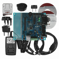
DEV KIT FOR C8051F320/F321
Manufacturer
Silicon Laboratories Inc
Type
MCUr
Specifications of C8051F320DK
Contents
Evaluation Board, Power Supply, USB Cables, Adapter and Documentation
Processor To Be Evaluated
C8051F320/F321
Interface Type
USB
Silicon Manufacturer
Silicon Labs
Core Architecture
8051
Silicon Core Number
C8051F320
Silicon Family Name
C8051F32x
Lead Free Status / RoHS Status
Contains lead / RoHS non-compliant
For Use With/related Products
Silicon Laboratories C8051F320, C8051F321
Lead Free Status / Rohs Status
Lead free / RoHS Compliant
Other names
336-1260
Available stocks
Company
Part Number
Manufacturer
Quantity
Price
Company:

Part Number:
C8051F320DK
Manufacturer:
SiliconL
Quantity:
4


C8051F320/1
11.4. Flash Write and Erase Guidelines
Any system which contains routines which write or erase Flash memory from software involves some risk
that the write or erase routines will execute unintentionally if the CPU is operating outside its specified
operating range of VDD, system clock frequency, or temperature. This accidental execution of Flash modi-
fying code can result in alteration of Flash memory contents causing a system failure that is only recover-
able by re-Flashing the code in the device.
To help prevent the accidental modification of Flash by firmware, the VDD Monitor must be enabled and
enabled as a reset source on C8051F32x devices for the Flash to be successfully modified. If either the
VDD Monitor or the VDD Monitor reset source is not enabled, a Flash Error Device Reset will be
generated when the firmware attempts to modify the Flash.
The following guidelines are recommended for any system that contains routines which write or erase
Flash from code.
11.4.1. VDD Maintenance and the VDD Monitor
110
1. If the system power supply is subject to voltage or current "spikes," add sufficient transient
2. Make certain that the minimum VDD rise time specification of 1 ms is met. If the system cannot
3. Keep the on-chip VDD Monitor enabled and enable the VDD Monitor as a reset source as
4. As an added precaution, explicitly enable the VDD Monitor and enable the VDD Monitor as a
5. Make certain that all writes to the RSTSRC (Reset Sources) register use direct assignment
6. Make certain that all writes to the RSTSRC register explicitly set the PORSF bit to a '1'. Areas
protection devices to the power supply to ensure that the supply voltages listed in the Absolute
Maximum Ratings table are not exceeded.
meet this rise time specification, then add an external VDD brownout circuit to the /RST pin of
the device that holds the device in reset until VDD reaches 2.7 V and re-asserts /RST if VDD
drops below 2.7 V.
early in code as possible. This should be the first set of instructions executed after the Reset
Vector. For 'C'-based systems, this will involve modifying the startup code added by the 'C'
compiler. See your compiler documentation for more details. Make certain that there are no
delays in software between enabling the VDD Monitor and enabling the VDD Monitor as a
reset source. Code examples showing this can be found in AN201, "Writing to Flash from
Firmware", available from the Silicon Laboratories web site.
reset source inside the functions that write and erase Flash memory. The VDD Monitor enable
instructions should be placed just after the instruction to set PSWE to a '1', but before the
Flash write or erase operation instruction.
operators and explicitly DO NOT use the bit-wise operators (such as AND or OR). For exam-
ple, "RSTSRC = 0x02" is correct, but "RSTSRC |= 0x02" is incorrect.
to check are initialization code which enables other reset sources, such as the Missing Clock
Detector or Comparator, for example, and instructions which force a Software Reset. A global
search on "RSTSRC" can quickly verify this.
Rev. 1.4
Related parts for C8051F320DK
Image
Part Number
Description
Manufacturer
Datasheet
Request
R

Part Number:
Description:
SMD/C°/SINGLE-ENDED OUTPUT SILICON OSCILLATOR
Manufacturer:
Silicon Laboratories Inc
Part Number:
Description:
Manufacturer:
Silicon Laboratories Inc
Datasheet:
Part Number:
Description:
N/A N/A/SI4010 AES KEYFOB DEMO WITH LCD RX
Manufacturer:
Silicon Laboratories Inc
Datasheet:
Part Number:
Description:
N/A N/A/SI4010 SIMPLIFIED KEY FOB DEMO WITH LED RX
Manufacturer:
Silicon Laboratories Inc
Datasheet:
Part Number:
Description:
N/A/-40 TO 85 OC/EZLINK MODULE; F930/4432 HIGH BAND (REV E/B1)
Manufacturer:
Silicon Laboratories Inc
Part Number:
Description:
EZLink Module; F930/4432 Low Band (rev e/B1)
Manufacturer:
Silicon Laboratories Inc
Part Number:
Description:
I°/4460 10 DBM RADIO TEST CARD 434 MHZ
Manufacturer:
Silicon Laboratories Inc
Part Number:
Description:
I°/4461 14 DBM RADIO TEST CARD 868 MHZ
Manufacturer:
Silicon Laboratories Inc
Part Number:
Description:
I°/4463 20 DBM RFSWITCH RADIO TEST CARD 460 MHZ
Manufacturer:
Silicon Laboratories Inc
Part Number:
Description:
I°/4463 20 DBM RADIO TEST CARD 868 MHZ
Manufacturer:
Silicon Laboratories Inc
Part Number:
Description:
I°/4463 27 DBM RADIO TEST CARD 868 MHZ
Manufacturer:
Silicon Laboratories Inc
Part Number:
Description:
I°/4463 SKYWORKS 30 DBM RADIO TEST CARD 915 MHZ
Manufacturer:
Silicon Laboratories Inc
Part Number:
Description:
N/A N/A/-40 TO 85 OC/4463 RFMD 30 DBM RADIO TEST CARD 915 MHZ
Manufacturer:
Silicon Laboratories Inc
Part Number:
Description:
I°/4463 20 DBM RADIO TEST CARD 169 MHZ
Manufacturer:
Silicon Laboratories Inc