C8051F320DK Silicon Laboratories Inc, C8051F320DK Datasheet - Page 133
C8051F320DK
Manufacturer Part Number
C8051F320DK
Description
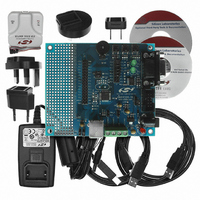
DEV KIT FOR C8051F320/F321
Manufacturer
Silicon Laboratories Inc
Type
MCUr
Specifications of C8051F320DK
Contents
Evaluation Board, Power Supply, USB Cables, Adapter and Documentation
Processor To Be Evaluated
C8051F320/F321
Interface Type
USB
Silicon Manufacturer
Silicon Labs
Core Architecture
8051
Silicon Core Number
C8051F320
Silicon Family Name
C8051F32x
Lead Free Status / RoHS Status
Contains lead / RoHS non-compliant
For Use With/related Products
Silicon Laboratories C8051F320, C8051F321
Lead Free Status / Rohs Status
Lead free / RoHS Compliant
Other names
336-1260
Available stocks
Company
Part Number
Manufacturer
Quantity
Price
Company:

Part Number:
C8051F320DK
Manufacturer:
SiliconL
Quantity:
4


Bits7–0: Output Configuration Bits for P0.7–P0.0 (respectively): ignored if corresponding bit in regis-
Bits7–0: P0.[7:0]
Bits7–0: Analog Input Configuration Bits for P0.7-P0.0 (respectively).
P0.7
R/W
R/W
R/W
Bit7
Bit7
Bit7
ter P0MDIN is logic 0.
0: Corresponding P0.n Output is open-drain.
1: Corresponding P0.n Output is push-pull.
(Note: When SDA and SCL appear on any of the Port I/O, each are open-drain regardless
of the value of P0MDOUT).
Write - Output appears on I/O pins per Crossbar Registers (when XBARE = ‘1’).
0: Logic Low Output.
1: Logic High Output (high impedance if corresponding P0MDOUT.n bit = 0).
Read - Always reads ‘0’ if selected as analog input in register P0MDIN. Directly reads Port
pin when configured as digital input.
0: P0.n pin is logic low.
1: P0.n pin is logic high.
Port pins configured as analog inputs have their weak pull-up, digital driver, and digital
receiver disabled.
0: Corresponding P0.n pin is configured as an analog input.
1: Corresponding P0.n pin is not configured as an analog input.
SFR Definition 14.5. P0MDOUT: Port0 Output Mode Register
P0.6
SFR Definition 14.4. P0MDIN: Port0 Input Mode Register
R/W
R/W
R/W
Bit6
Bit6
Bit6
SFR Definition 14.3. P0: Port0 Register
P0.5
R/W
R/W
R/W
Bit5
Bit5
Bit5
P0.4
R/W
R/W
R/W
Bit4
Bit4
Bit4
Rev. 1.4
P0.3
R/W
R/W
R/W
Bit3
Bit3
Bit3
P0.2
R/W
R/W
R/W
Bit2
Bit2
Bit2
P0.1
R/W
R/W
R/W
Bit1
Bit1
Bit1
C8051F320/1
(bit addressable)
P0.0
R/W
R/W
R/W
Bit0
Bit0
Bit0
SFR Address:
SFR Address:
SFR Address:
00000000
Reset Value
Reset Value
Reset Value
11111111
11111111
0xA4
0x80
0xF1
133
Related parts for C8051F320DK
Image
Part Number
Description
Manufacturer
Datasheet
Request
R

Part Number:
Description:
SMD/C°/SINGLE-ENDED OUTPUT SILICON OSCILLATOR
Manufacturer:
Silicon Laboratories Inc
Part Number:
Description:
Manufacturer:
Silicon Laboratories Inc
Datasheet:
Part Number:
Description:
N/A N/A/SI4010 AES KEYFOB DEMO WITH LCD RX
Manufacturer:
Silicon Laboratories Inc
Datasheet:
Part Number:
Description:
N/A N/A/SI4010 SIMPLIFIED KEY FOB DEMO WITH LED RX
Manufacturer:
Silicon Laboratories Inc
Datasheet:
Part Number:
Description:
N/A/-40 TO 85 OC/EZLINK MODULE; F930/4432 HIGH BAND (REV E/B1)
Manufacturer:
Silicon Laboratories Inc
Part Number:
Description:
EZLink Module; F930/4432 Low Band (rev e/B1)
Manufacturer:
Silicon Laboratories Inc
Part Number:
Description:
I°/4460 10 DBM RADIO TEST CARD 434 MHZ
Manufacturer:
Silicon Laboratories Inc
Part Number:
Description:
I°/4461 14 DBM RADIO TEST CARD 868 MHZ
Manufacturer:
Silicon Laboratories Inc
Part Number:
Description:
I°/4463 20 DBM RFSWITCH RADIO TEST CARD 460 MHZ
Manufacturer:
Silicon Laboratories Inc
Part Number:
Description:
I°/4463 20 DBM RADIO TEST CARD 868 MHZ
Manufacturer:
Silicon Laboratories Inc
Part Number:
Description:
I°/4463 27 DBM RADIO TEST CARD 868 MHZ
Manufacturer:
Silicon Laboratories Inc
Part Number:
Description:
I°/4463 SKYWORKS 30 DBM RADIO TEST CARD 915 MHZ
Manufacturer:
Silicon Laboratories Inc
Part Number:
Description:
N/A N/A/-40 TO 85 OC/4463 RFMD 30 DBM RADIO TEST CARD 915 MHZ
Manufacturer:
Silicon Laboratories Inc
Part Number:
Description:
I°/4463 20 DBM RADIO TEST CARD 169 MHZ
Manufacturer:
Silicon Laboratories Inc