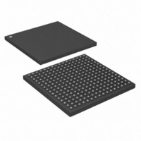
DS26518GNB1+ Maxim Integrated Products, DS26518GNB1+ Datasheet - Page 92

DS26518GNB1+
Manufacturer Part Number
DS26518GNB1+
Description
IC TXRX T1/E1/J1 8PRT 256-CSBGA
Manufacturer
Maxim Integrated Products
Type
Transceiverr
Datasheet
1.DS26518GNB1.pdf
(312 pages)
Specifications of DS26518GNB1+
Number Of Drivers/receivers
8/8
Protocol
T1/E1/J1
Voltage - Supply
3.135 V ~ 3.465 V
Mounting Type
Surface Mount
Package / Case
256-CSBGA
Lead Free Status / RoHS Status
Lead free / RoHS Compliant
- Current page: 92 of 312
- Download datasheet (3Mb)
Figure 9-24. Receive LIU Termination Options
The device couples to the receive E1 or T1 twisted pair (or coaxial cable in 75Ω E1 applications) via a 1:1 or 2:1
transformer. See
Receive sensitivity is configurable by setting the appropriate RSMS[1:0] bits (LRCR).
The DS26518 uses a digital clock recovery system. The resultant E1, T1 or J1 clock derived from MCLK is
multiplied by 16 via an internal PLL and fed to the clock recovery system. The clock recovery system uses the
clock from the PLL circuit to form a 16 times oversampler, which is used to recover the clock and data. This
oversampling technique offers outstanding performance to meet jitter tolerance specifications shown in
Figure
Normally, the clock that is output at the RCLKn pin is the recovered clock from the E1 AMI/HDB3 or T1 AMI/B8ZS
waveform presented at the RTIPn and RRINGn inputs. If the jitter attenuator (LTRCR) is placed in the receive path
(as is the case in most applications), the jitter attenuator restores the RCLKn to an approximate 50% duty cycle. If
the jitter attenuator is either placed in the transmit path or is disabled, the RCLKn output can exhibit slightly shorter
high cycles of the clock. This is due to the highly over-sampled digital clock recovery circuitry. See
more details. When no signal is present at RTIPn and RRINGn, a receive carrier loss (RCL) condition will occur
and the RCLKn will be derived from the MCLKT1 or MCLKE1 source (depending on the configuration).
9.12.3.2
The DS26518 will report the signal strength at RTIPn and RRINGn in approximately 2.5dB increments via RSL[3:0]
located in the LIU Receive Signal Level Register (LRSL). This feature is helpful when trouble shooting line
performance problems.
9.12.3.3
The DS26518 can receive a 2.048MHz square-wave synchronization clock as specified in Section 10 of ITU-T
G.703. To use this mode, set the receive G.703 clock bit (RG703) found in the LIU Receive Control Register
(LRCR.7).
9-27.
Receive Level Indicator
Receive G.703 Section 10 Synchronization Signal
Table 9-42
RECEIVE LIU
R
T
for transformer details.
R
T
RRINGn
RTIPn
LRISMR.RIMPON
92 of 312
TFR
1:1
Rx LINE
Table 13-3
for
Related parts for DS26518GNB1+
Image
Part Number
Description
Manufacturer
Datasheet
Request
R

Part Number:
Description:
8-port T1/e1/j1 Transceiver
Manufacturer:
Maxim Integrated Products, Inc.
Datasheet:

Part Number:
Description:
Ds26518 8-port T1/e1/j1 Transceiver
Manufacturer:
Maxim Integrated Products, Inc.

Part Number:
Description:
MAX7528KCWPMaxim Integrated Products [CMOS Dual 8-Bit Buffered Multiplying DACs]
Manufacturer:
Maxim Integrated Products
Datasheet:

Part Number:
Description:
Single +5V, fully integrated, 1.25Gbps laser diode driver.
Manufacturer:
Maxim Integrated Products
Datasheet:

Part Number:
Description:
Single +5V, fully integrated, 155Mbps laser diode driver.
Manufacturer:
Maxim Integrated Products
Datasheet:

Part Number:
Description:
VRD11/VRD10, K8 Rev F 2/3/4-Phase PWM Controllers with Integrated Dual MOSFET Drivers
Manufacturer:
Maxim Integrated Products
Datasheet:

Part Number:
Description:
Highly Integrated Level 2 SMBus Battery Chargers
Manufacturer:
Maxim Integrated Products
Datasheet:

Part Number:
Description:
Current Monitor and Accumulator with Integrated Sense Resistor; ; Temperature Range: -40°C to +85°C
Manufacturer:
Maxim Integrated Products

Part Number:
Description:
TSSOP 14/A°/RS-485 Transceivers with Integrated 100O/120O Termination Resis
Manufacturer:
Maxim Integrated Products

Part Number:
Description:
TSSOP 14/A°/RS-485 Transceivers with Integrated 100O/120O Termination Resis
Manufacturer:
Maxim Integrated Products

Part Number:
Description:
QFN 16/A°/AC-DC and DC-DC Peak-Current-Mode Converters with Integrated Step
Manufacturer:
Maxim Integrated Products

Part Number:
Description:
TDFN/A/65V, 1A, 600KHZ, SYNCHRONOUS STEP-DOWN REGULATOR WITH INTEGRATED SWI
Manufacturer:
Maxim Integrated Products

Part Number:
Description:
Integrated Temperature Controller f
Manufacturer:
Maxim Integrated Products

Part Number:
Description:
SOT23-6/I°/45MHz to 650MHz, Integrated IF VCOs with Differential Output
Manufacturer:
Maxim Integrated Products

Part Number:
Description:
SOT23-6/I°/45MHz to 650MHz, Integrated IF VCOs with Differential Output
Manufacturer:
Maxim Integrated Products


