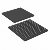
DS26518GNB1+ Maxim Integrated Products, DS26518GNB1+ Datasheet - Page 293

DS26518GNB1+
Manufacturer Part Number
DS26518GNB1+
Description
IC TXRX T1/E1/J1 8PRT 256-CSBGA
Manufacturer
Maxim Integrated Products
Type
Transceiverr
Datasheet
1.DS26518GNB1.pdf
(312 pages)
Specifications of DS26518GNB1+
Number Of Drivers/receivers
8/8
Protocol
T1/E1/J1
Voltage - Supply
3.135 V ~ 3.465 V
Mounting Type
Surface Mount
Package / Case
256-CSBGA
Lead Free Status / RoHS Status
Lead free / RoHS Compliant
- Current page: 293 of 312
- Download datasheet (3Mb)
Note 1:
Note 2:
Note 3:
Note 4:
13.
Unless otherwise noted, all timing numbers assume 20pF test load on output signals, 40pF test load on bus
signals.
13.1
13.1.1 SPI Bus Mode
Table 13-1. SPI Bus Mode Timing
(See
SYMBOL
(Note 1)
t4, t5
t10
Figure
t1
t2
t3
t6
t7
t8
t9
AC TIMING CHARACTERISTICS
Microprocessor Bus AC Characteristics
Symbols refer to dimensions in
100pF load on all SPI pins.
Hold time to high-impedance state.
With 100pF on all SPI pins.
13-1.)
Operating Frequency
Slave
Cycle Time: Slave
Enable Lead Time
Enable Lag Time
Clock (CLK) Duty Cycle
Slave (t4/t1 or t5/t1)
Data Setup Time (Inputs)
Slave
Data Hold Time (Inputs)
Slave
Disable Time, Slave (Note 3)
Data Valid Time, After Enable Edge
Slave (Note 4)
Data Hold Time, Outputs, After Enable Edge
Slave
CHARACTERISTIC (Note 2)
Figure
13-1.
293 of 312
SYMBOL
f
t
t
t
t
BUS(S)
CLKH(S)
LEAD(S)
t
t
CYC(S)
t
LAG(S)
t
DIS(S)
t
HD(S)
SU(S)
H(S)
V(S)
MIN
200
15
15
80
15
5
5
MAX
25
40
5
UNITS
MHz
ns
ns
ns
ns
ns
ns
ns
ns
ns
Related parts for DS26518GNB1+
Image
Part Number
Description
Manufacturer
Datasheet
Request
R

Part Number:
Description:
8-port T1/e1/j1 Transceiver
Manufacturer:
Maxim Integrated Products, Inc.
Datasheet:

Part Number:
Description:
Ds26518 8-port T1/e1/j1 Transceiver
Manufacturer:
Maxim Integrated Products, Inc.

Part Number:
Description:
MAX7528KCWPMaxim Integrated Products [CMOS Dual 8-Bit Buffered Multiplying DACs]
Manufacturer:
Maxim Integrated Products
Datasheet:

Part Number:
Description:
Single +5V, fully integrated, 1.25Gbps laser diode driver.
Manufacturer:
Maxim Integrated Products
Datasheet:

Part Number:
Description:
Single +5V, fully integrated, 155Mbps laser diode driver.
Manufacturer:
Maxim Integrated Products
Datasheet:

Part Number:
Description:
VRD11/VRD10, K8 Rev F 2/3/4-Phase PWM Controllers with Integrated Dual MOSFET Drivers
Manufacturer:
Maxim Integrated Products
Datasheet:

Part Number:
Description:
Highly Integrated Level 2 SMBus Battery Chargers
Manufacturer:
Maxim Integrated Products
Datasheet:

Part Number:
Description:
Current Monitor and Accumulator with Integrated Sense Resistor; ; Temperature Range: -40°C to +85°C
Manufacturer:
Maxim Integrated Products

Part Number:
Description:
TSSOP 14/A°/RS-485 Transceivers with Integrated 100O/120O Termination Resis
Manufacturer:
Maxim Integrated Products

Part Number:
Description:
TSSOP 14/A°/RS-485 Transceivers with Integrated 100O/120O Termination Resis
Manufacturer:
Maxim Integrated Products

Part Number:
Description:
QFN 16/A°/AC-DC and DC-DC Peak-Current-Mode Converters with Integrated Step
Manufacturer:
Maxim Integrated Products

Part Number:
Description:
TDFN/A/65V, 1A, 600KHZ, SYNCHRONOUS STEP-DOWN REGULATOR WITH INTEGRATED SWI
Manufacturer:
Maxim Integrated Products

Part Number:
Description:
Integrated Temperature Controller f
Manufacturer:
Maxim Integrated Products

Part Number:
Description:
SOT23-6/I°/45MHz to 650MHz, Integrated IF VCOs with Differential Output
Manufacturer:
Maxim Integrated Products

Part Number:
Description:
SOT23-6/I°/45MHz to 650MHz, Integrated IF VCOs with Differential Output
Manufacturer:
Maxim Integrated Products


