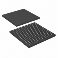
DS26518GNB1+ Maxim Integrated Products, DS26518GNB1+ Datasheet - Page 80

DS26518GNB1+
Manufacturer Part Number
DS26518GNB1+
Description
IC TXRX T1/E1/J1 8PRT 256-CSBGA
Manufacturer
Maxim Integrated Products
Type
Transceiverr
Datasheet
1.DS26518GNB1.pdf
(312 pages)
Specifications of DS26518GNB1+
Number Of Drivers/receivers
8/8
Protocol
T1/E1/J1
Voltage - Supply
3.135 V ~ 3.465 V
Mounting Type
Surface Mount
Package / Case
256-CSBGA
Lead Free Status / RoHS Status
Lead free / RoHS Compliant
- Current page: 80 of 312
- Download datasheet (3Mb)
9.10.3 HDLC-256 Controller
This device has an enhanced HDLC controller that can be mapped into up to 32 time slots, or Sa4 to Sa8 bits (E1
mode), or the FDL (T1 mode). This HDLC controller has a 256-byte FIFO buffer in both the transmit and receive
paths. The user can select any specific bits within the time slot(s) to assign to the HDLC-256 controller as well as
specific Sa bits (E1 mode).
The HDLC-256 controller performs all the necessary overhead for generating and receiving performance report
messages (PRMs) as described in ANSI T1.403 and the messages as described in AT&T TR54016. The
HDLC-256 controller automatically generates and detects flags, generates and checks the CRC checksum,
generates and detects abort sequences, stuffs and destuffs zeros, and byte aligns to the data stream. The
256-byte buffers in the HDLC-256 controller are large enough to allow a full PRM to be received or transmitted
without host intervention. They are also large enough to store an entire frame’s worth of data before requiring host
intervention.
Table 9-38
Table 9-38. Registers Related to the HDLC-256
Receive Expansion Port Control Register
(HDLC-256) (RXPC)
Receive HDLC-256 Channel Select
Registers 1 to 4(RHCS1–RHCS4)
Receive HDLC-256 Bit Suppress Register
(RHBS)
Receive HDLC-256 Control Register 1
(RH256CR1)
Receive HDLC-256 Control Register 2
(RH256CR2)
Receive HDLC-256 Status Register
(RH256SR)
Receive HDLC-256 FIFO Data Registers
1 and 2
Transmit Expansion Port Control Register
(TXPC)
Transmit HDLC-256 Channel Select
Registers 1 to 4 (THCS1–THCS4)
Transmit HDLC-256 Bit Suppress
Register (THBS)
Transmit HDLC-256 Control Register 1
(TH256CR1)
Transmit HDLC-256 Control Register 2
(TH256CR2)
Transmit HDLC-256 FIFO Data Registers
1 and 2
Transmit HDLC-256 Status Registers 1
and 2
Note: The addresses shown are for Framer 1. Addresses for Framers 2 to 8 can be calculated using the following: Framer n = (Framer 1
address + (n - 1) x 200hex); where n = 2 to 8 for Framers 2 to 8.
(TH256SR1
(RH256FDR1
(TH256FDR1
shows the registers related to the HDLC-256.
REGISTER
and TH256SR2)
and TH256FDR2)
and RH256FDR2)
0DCh, 0DDh, 0DEh,
1DCh, 1DDh, 1DEh,
151Ch, 151Dh
ADDRESSES
1502h, 1503h
1504h, 1505h
FRAMER 1
1510h
1511h
1514h
1500h
1501h
0DFh
08Dh
1DFh
18Dh
80 of 312
08Ah
18Ah
Mapping of the HDLC-256 to time slots or FDL,
Sa bits.
Selection of time slots to map data to the
HDLC-256 port.
Receive HDLC-256 bit suppression register.
Receive miscellaneous control.
Receive HDLC-256 FIFO data level available.
Indicates the FIFO status.
The actual FIFO data.
Mapping of the HDLC-256 to time slots or FDL,
Sa bits.
Selection of time slots to map data from the
HDLC-256 port.
Transmit HDLC-256 bit suppress for bits not to
be used.
Transmit miscellaneous control.
Indicates the number of bytes that can be
written into the transmit FIFO.
Transmit HDLC-256 FIFO.
Indicates the real-time status of the transmit
HDLC-256 FIFO.
FUNCTION
Related parts for DS26518GNB1+
Image
Part Number
Description
Manufacturer
Datasheet
Request
R

Part Number:
Description:
8-port T1/e1/j1 Transceiver
Manufacturer:
Maxim Integrated Products, Inc.
Datasheet:

Part Number:
Description:
Ds26518 8-port T1/e1/j1 Transceiver
Manufacturer:
Maxim Integrated Products, Inc.

Part Number:
Description:
MAX7528KCWPMaxim Integrated Products [CMOS Dual 8-Bit Buffered Multiplying DACs]
Manufacturer:
Maxim Integrated Products
Datasheet:

Part Number:
Description:
Single +5V, fully integrated, 1.25Gbps laser diode driver.
Manufacturer:
Maxim Integrated Products
Datasheet:

Part Number:
Description:
Single +5V, fully integrated, 155Mbps laser diode driver.
Manufacturer:
Maxim Integrated Products
Datasheet:

Part Number:
Description:
VRD11/VRD10, K8 Rev F 2/3/4-Phase PWM Controllers with Integrated Dual MOSFET Drivers
Manufacturer:
Maxim Integrated Products
Datasheet:

Part Number:
Description:
Highly Integrated Level 2 SMBus Battery Chargers
Manufacturer:
Maxim Integrated Products
Datasheet:

Part Number:
Description:
Current Monitor and Accumulator with Integrated Sense Resistor; ; Temperature Range: -40°C to +85°C
Manufacturer:
Maxim Integrated Products

Part Number:
Description:
TSSOP 14/A°/RS-485 Transceivers with Integrated 100O/120O Termination Resis
Manufacturer:
Maxim Integrated Products

Part Number:
Description:
TSSOP 14/A°/RS-485 Transceivers with Integrated 100O/120O Termination Resis
Manufacturer:
Maxim Integrated Products

Part Number:
Description:
QFN 16/A°/AC-DC and DC-DC Peak-Current-Mode Converters with Integrated Step
Manufacturer:
Maxim Integrated Products

Part Number:
Description:
TDFN/A/65V, 1A, 600KHZ, SYNCHRONOUS STEP-DOWN REGULATOR WITH INTEGRATED SWI
Manufacturer:
Maxim Integrated Products

Part Number:
Description:
Integrated Temperature Controller f
Manufacturer:
Maxim Integrated Products

Part Number:
Description:
SOT23-6/I°/45MHz to 650MHz, Integrated IF VCOs with Differential Output
Manufacturer:
Maxim Integrated Products

Part Number:
Description:
SOT23-6/I°/45MHz to 650MHz, Integrated IF VCOs with Differential Output
Manufacturer:
Maxim Integrated Products


