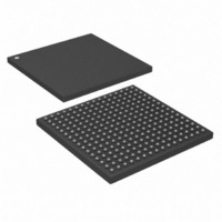
DS26518GNB1+ Maxim Integrated Products, DS26518GNB1+ Datasheet - Page 130

DS26518GNB1+
Manufacturer Part Number
DS26518GNB1+
Description
IC TXRX T1/E1/J1 8PRT 256-CSBGA
Manufacturer
Maxim Integrated Products
Type
Transceiverr
Datasheet
1.DS26518GNB1.pdf
(312 pages)
Specifications of DS26518GNB1+
Number Of Drivers/receivers
8/8
Protocol
T1/E1/J1
Voltage - Supply
3.135 V ~ 3.465 V
Mounting Type
Surface Mount
Package / Case
256-CSBGA
Lead Free Status / RoHS Status
Lead free / RoHS Compliant
- Current page: 130 of 312
- Download datasheet (3Mb)
Register Name:
Description:
Register Address:
Bit #
Name
Default
Bits 7 and 6: Interleave Bus Operation Mode Select 1 and 0 (IBOMS[1:0]). These bits determine the
configuration of the IBO (interleaved bus) multiplexer and inform the framers of the IBO configuration. These bits
should be used in conjunction with the Rx and Tx IBO control registers within each of the framer units. These bits
control Channels 1 to 8. Additional information concerning the IBO multiplexer is given in Section 9.8.2. These bits
must be set whether using the internal IBO mux or externally ganging the pins.
Bits 5 and 4: Backplane Clock Select 1 and 0 (BPCLK[1:0]). These bits determine the clock frequency output on
the BPCLK1 pin.
Bit 2: Receive Frame/Multiframe Sync Select (RFMSS). This bit controls the function of all eight
RMSYNCn/RFSYNCn pins.
Bit 1: Transmit Channel Block/Clock Select (TCBCS). This bit controls the function of all eight
TCHBLKn/TCHCLKn pins.
Bit 0: Receive Channel Block/Clock Select (RCBCS). This bit controls the function of all eight
RCHBLKn/RCHCLKn pins.
BPCLK1
IBOMS1
0
0
1
1
0
0
1
1
0 = RMSYNC/RFSYNC[8:1] pins output RFSYNC[8:1] (Receive Frame Sync)
1 = RMSYNC/RFSYNC[8:1] pins output RMSYNC[8:1] (Receive Multiframe Sync)
0 = TCHBLK/TCHCLK[8:1] pins output TCHBLK[8:1] (Transmit Channel Block)
1 = TCHBLK/TCHCLK[8:1] pins output TCHCLK[8:1] (Transmit Channel Clock)
0 = RCHBLK/RCHCLK[8:1] pins output RCHBLK[8:1] (Receive Channel Block)
1 = RCHBLK/RCHCLK[8:1] pins output RCHCLK[8:1] (Receive Channel Clock)
IBOMS1
7
0
BPCLK0
IBOMS0
0
1
0
1
0
1
0
1
IBOMS0
GFCR1
Global Framer Control Register 1
00F1h
6
0
IBO disabled.
2 devices on bus (4.096MHz).
4 devices on bus (8.192MHz).
8 devices on bus (16.384MHz).
BPCLK1 Frequency
BPCLK1
16.384MHz
5
0
IBO Mode
2.048MHz
4.096MHz
8.192MHz
BPCLK0
130 of 312
4
0
—
3
0
RFMSS
2
0
TCBCS
1
0
RCBCS
0
0
Related parts for DS26518GNB1+
Image
Part Number
Description
Manufacturer
Datasheet
Request
R

Part Number:
Description:
8-port T1/e1/j1 Transceiver
Manufacturer:
Maxim Integrated Products, Inc.
Datasheet:

Part Number:
Description:
Ds26518 8-port T1/e1/j1 Transceiver
Manufacturer:
Maxim Integrated Products, Inc.

Part Number:
Description:
MAX7528KCWPMaxim Integrated Products [CMOS Dual 8-Bit Buffered Multiplying DACs]
Manufacturer:
Maxim Integrated Products
Datasheet:

Part Number:
Description:
Single +5V, fully integrated, 1.25Gbps laser diode driver.
Manufacturer:
Maxim Integrated Products
Datasheet:

Part Number:
Description:
Single +5V, fully integrated, 155Mbps laser diode driver.
Manufacturer:
Maxim Integrated Products
Datasheet:

Part Number:
Description:
VRD11/VRD10, K8 Rev F 2/3/4-Phase PWM Controllers with Integrated Dual MOSFET Drivers
Manufacturer:
Maxim Integrated Products
Datasheet:

Part Number:
Description:
Highly Integrated Level 2 SMBus Battery Chargers
Manufacturer:
Maxim Integrated Products
Datasheet:

Part Number:
Description:
Current Monitor and Accumulator with Integrated Sense Resistor; ; Temperature Range: -40°C to +85°C
Manufacturer:
Maxim Integrated Products

Part Number:
Description:
TSSOP 14/A°/RS-485 Transceivers with Integrated 100O/120O Termination Resis
Manufacturer:
Maxim Integrated Products

Part Number:
Description:
TSSOP 14/A°/RS-485 Transceivers with Integrated 100O/120O Termination Resis
Manufacturer:
Maxim Integrated Products

Part Number:
Description:
QFN 16/A°/AC-DC and DC-DC Peak-Current-Mode Converters with Integrated Step
Manufacturer:
Maxim Integrated Products

Part Number:
Description:
TDFN/A/65V, 1A, 600KHZ, SYNCHRONOUS STEP-DOWN REGULATOR WITH INTEGRATED SWI
Manufacturer:
Maxim Integrated Products

Part Number:
Description:
Integrated Temperature Controller f
Manufacturer:
Maxim Integrated Products

Part Number:
Description:
SOT23-6/I°/45MHz to 650MHz, Integrated IF VCOs with Differential Output
Manufacturer:
Maxim Integrated Products

Part Number:
Description:
SOT23-6/I°/45MHz to 650MHz, Integrated IF VCOs with Differential Output
Manufacturer:
Maxim Integrated Products


