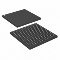
DS26518GNB1+ Maxim Integrated Products, DS26518GNB1+ Datasheet - Page 20

DS26518GNB1+
Manufacturer Part Number
DS26518GNB1+
Description
IC TXRX T1/E1/J1 8PRT 256-CSBGA
Manufacturer
Maxim Integrated Products
Type
Transceiverr
Datasheet
1.DS26518GNB1.pdf
(312 pages)
Specifications of DS26518GNB1+
Number Of Drivers/receivers
8/8
Protocol
T1/E1/J1
Voltage - Supply
3.135 V ~ 3.465 V
Mounting Type
Surface Mount
Package / Case
256-CSBGA
Lead Free Status / RoHS Status
Lead free / RoHS Compliant
- Current page: 20 of 312
- Download datasheet (3Mb)
8.
8.1
Table 8-1. Detailed Pin Descriptions
TXENABLE/
SCAN_EN
RESREF
RRING1
RRING2
RRING3
RRING4
RRING5
RRING6
RRING7
RRING8
TRING1
TRING2
TRING3
TRING4
TRING5
TRING6
TRING7
TRING8
NAME
RTIP1
RTIP2
RTIP3
RTIP4
RTIP5
RTIP6
RTIP7
RTIP8
TTIP1
TTIP2
TTIP3
TTIP4
TTIP5
TTIP6
TTIP7
TTIP8
PIN DESCRIPTIONS
Pin Functional Description
H15, H16
G14, H14
A15, A16
A14, B14
T15, T16
R14,T14
J14, K14
J15, J16
H1, H2
G3, H3
A1, A2
A3, B3
R3, T3
T1, T2
J3, K3
J1 J2
C16
C15
P16
F16
P15
F15
PIN
L13
L16
L15
C1
P1
C2
P2
F1
L1
F2
L2
J5
Impedance
Impedance
Output,
Output,
Analog
Analog
Analog
Analog
TYPE
Input
Input
Input
Input
High
High
Transmit Bipolar Tip for Transceiver 1 to 8. These pins are differential line
driver tip outputs. These pins can be high impedance if:
If TXENABLE is low, TTIPn/TRINGn will be high impedance. Note that if
TXENABLE is low, the register settings for control of TTIPn/TRINGn are ignored
and output is high impedance.
The differential outputs of TTIPn and TRINGn can provide internal matched
impedance for E1 75Ω, E1 120Ω, T1 100Ω, or J1 110Ω. The user can turn off
internal termination.
Note: The two pins shown for each transmit bipolar tip (e.g., pins A1 and A2 for
TTIP1) should be tied together.
Transmit Bipolar Ring for Transceiver 1 to 8. These pins are differential line
driver ring outputs. These pins can be high impedance if:
If TXENABLE is low, TTIPn/TRINGn will be high impedance. Note that if
TXENABLE is low, the register settings for control of TTIPn/TRINGn are ignored
and output is high impedance.
The differential outputs of TTIPn and TRINGn can provide internal matched
impedance for E1 75Ω, E1 120Ω, T1 100Ω, or J1 110Ω. The user can turn off
internal termination.
Note: The two pins shown for each transmit bipolar ring (e.g., pins A3 and B3 for
TRING1) should be tied together.
Transmit Enable. If this pin is pulled low, all transmitter outputs (TTIPn and
TRINGn) are high impedance. The register settings for tri-state control of
TTIPn/TRINGn are ignored if TXENABLE is low. If TXENABLE is high, the
particular driver can be tri-stated by the register settings.
Scan Enable. When low, device is in normal operation. Scan enable is selected
by the SCANMODE pin. Note: User should not select scan enable—test mode
only.
Receive Bipolar Tip for Transceiver 1 to 8. The differential inputs of RTIPn
and RRINGn can provide internal matched impedance for E1 75Ω, E1 120Ω, T1
100Ω, or J1 110Ω. The user can turn off internal termination via the LIU Receive
Impedance and Sensitivity Monitor register (LRISMR).
Receive Bipolar Ring for Transceiver 1 to 8. The differential inputs of RTIPn
and RRINGn can provide internal matched impedance for E1 75Ω, E1 120Ω, T1
100Ω, or J1 110Ω. The user has the option of turning off internal termination via
the LIU Receive Impedance and Sensitivity Monitor register (LRISMR).
Resistor Reference. This pin is used to calibrate the internal impedance match
resistors of the receive LIUs. This pin should be tied to V
resistor.
ANALOG TRANSMIT
ANALOG RECEIVE
20 of 312
FUNCTION
SS
through a 10kΩ ±1%
Related parts for DS26518GNB1+
Image
Part Number
Description
Manufacturer
Datasheet
Request
R

Part Number:
Description:
8-port T1/e1/j1 Transceiver
Manufacturer:
Maxim Integrated Products, Inc.
Datasheet:

Part Number:
Description:
Ds26518 8-port T1/e1/j1 Transceiver
Manufacturer:
Maxim Integrated Products, Inc.

Part Number:
Description:
MAX7528KCWPMaxim Integrated Products [CMOS Dual 8-Bit Buffered Multiplying DACs]
Manufacturer:
Maxim Integrated Products
Datasheet:

Part Number:
Description:
Single +5V, fully integrated, 1.25Gbps laser diode driver.
Manufacturer:
Maxim Integrated Products
Datasheet:

Part Number:
Description:
Single +5V, fully integrated, 155Mbps laser diode driver.
Manufacturer:
Maxim Integrated Products
Datasheet:

Part Number:
Description:
VRD11/VRD10, K8 Rev F 2/3/4-Phase PWM Controllers with Integrated Dual MOSFET Drivers
Manufacturer:
Maxim Integrated Products
Datasheet:

Part Number:
Description:
Highly Integrated Level 2 SMBus Battery Chargers
Manufacturer:
Maxim Integrated Products
Datasheet:

Part Number:
Description:
Current Monitor and Accumulator with Integrated Sense Resistor; ; Temperature Range: -40°C to +85°C
Manufacturer:
Maxim Integrated Products

Part Number:
Description:
TSSOP 14/A°/RS-485 Transceivers with Integrated 100O/120O Termination Resis
Manufacturer:
Maxim Integrated Products

Part Number:
Description:
TSSOP 14/A°/RS-485 Transceivers with Integrated 100O/120O Termination Resis
Manufacturer:
Maxim Integrated Products

Part Number:
Description:
QFN 16/A°/AC-DC and DC-DC Peak-Current-Mode Converters with Integrated Step
Manufacturer:
Maxim Integrated Products

Part Number:
Description:
TDFN/A/65V, 1A, 600KHZ, SYNCHRONOUS STEP-DOWN REGULATOR WITH INTEGRATED SWI
Manufacturer:
Maxim Integrated Products

Part Number:
Description:
Integrated Temperature Controller f
Manufacturer:
Maxim Integrated Products

Part Number:
Description:
SOT23-6/I°/45MHz to 650MHz, Integrated IF VCOs with Differential Output
Manufacturer:
Maxim Integrated Products

Part Number:
Description:
SOT23-6/I°/45MHz to 650MHz, Integrated IF VCOs with Differential Output
Manufacturer:
Maxim Integrated Products


