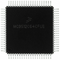
MC9S12C64CFUE Freescale Semiconductor, MC9S12C64CFUE Datasheet - Page 165

MC9S12C64CFUE
Manufacturer Part Number
MC9S12C64CFUE
Description
IC MCU 64K FLASH 4K RAM 80-QFP
Manufacturer
Freescale Semiconductor
Series
HCS12r
Specifications of MC9S12C64CFUE
Core Processor
HCS12
Core Size
16-Bit
Speed
25MHz
Connectivity
CAN, EBI/EMI, SCI, SPI
Peripherals
POR, PWM, WDT
Number Of I /o
60
Program Memory Size
64KB (64K x 8)
Program Memory Type
FLASH
Ram Size
4K x 8
Voltage - Supply (vcc/vdd)
2.35 V ~ 5.5 V
Data Converters
A/D 8x10b
Oscillator Type
Internal
Operating Temperature
-40°C ~ 85°C
Package / Case
80-QFP
Processor Series
S12C
Core
HCS12
Data Bus Width
16 bit
Data Ram Size
4 KB
Interface Type
CAN/SCI/SPI
Maximum Clock Frequency
25 MHz
Number Of Programmable I/os
60
Number Of Timers
8
Maximum Operating Temperature
+ 85 C
Mounting Style
SMD/SMT
3rd Party Development Tools
EWHCS12
Development Tools By Supplier
M68EVB912C32EE
Minimum Operating Temperature
- 40 C
On-chip Adc
8-ch x 10-bit
Package
80PQFP
Family Name
HCS12
Maximum Speed
25 MHz
Operating Supply Voltage
2.5|5 V
Height
2.4 mm
Length
14 mm
Supply Voltage (max)
2.75 V, 5.5 V
Supply Voltage (min)
2.35 V, 2.97 V
Width
14 mm
Lead Free Status / RoHS Status
Lead free / RoHS Compliant
Eeprom Size
-
Lead Free Status / Rohs Status
Lead free / RoHS Compliant
Available stocks
Company
Part Number
Manufacturer
Quantity
Price
Company:
Part Number:
MC9S12C64CFUE
Manufacturer:
Freescale Semiconductor
Quantity:
10 000
- Current page: 165 of 690
- Download datasheet (4Mb)
Chapter 6
Background Debug Module (BDMV4) Block Description
6.1
This section describes the functionality of the background debug module (BDM) sub-block of the HCS12
core platform.
A block diagram of the BDM is shown in
The background debug module (BDM) sub-block is a single-wire, background debug system implemented
in on-chip hardware for minimal CPU intervention. All interfacing with the BDM is done via the BKGD
pin.
BDMV4 has enhanced capability for maintaining synchronization between the target and host while
allowing more flexibility in clock rates. This includes a sync signal to show the clock rate and a handshake
signal to indicate when an operation is complete. The system is backwards compatible with older external
interfaces.
6.1.1
Freescale Semiconductor
•
•
•
•
•
•
Single-wire communication with host development system
BDMV4 (and BDM2): Enhanced capability for allowing more flexibility in clock rates
BDMV4: SYNC command to determine communication rate
BDMV4: GO_UNTIL command
BDMV4: Hardware handshake protocol to increase the performance of the serial communication
Active out of reset in special single-chip mode
Introduction
Features
SYSTEM
HOST
BDMACT
ENBDM
ENTAG
TRACE
SDV
BKGD
16-BIT SHIFT REGISTER
INSTRUCTION DECODE
MC9S12C-Family / MC9S12GC-Family
Figure 6-1. BDM Block Diagram
AND EXECUTION
STANDARD BDM
LOOKUP TABLE
FIRMWARE
Figure
Rev 01.24
6-1.
CONTROL LOGIC
BUS INTERFACE
CLKSW
AND
ADDRESS
DATA
CLOCKS
165
Related parts for MC9S12C64CFUE
Image
Part Number
Description
Manufacturer
Datasheet
Request
R
Part Number:
Description:
Manufacturer:
Freescale Semiconductor, Inc
Datasheet:
Part Number:
Description:
Manufacturer:
Freescale Semiconductor, Inc
Datasheet:
Part Number:
Description:
Manufacturer:
Freescale Semiconductor, Inc
Datasheet:
Part Number:
Description:
Manufacturer:
Freescale Semiconductor, Inc
Datasheet:
Part Number:
Description:
Manufacturer:
Freescale Semiconductor, Inc
Datasheet:
Part Number:
Description:
Manufacturer:
Freescale Semiconductor, Inc
Datasheet:
Part Number:
Description:
Manufacturer:
Freescale Semiconductor, Inc
Datasheet:
Part Number:
Description:
Manufacturer:
Freescale Semiconductor, Inc
Datasheet:
Part Number:
Description:
Manufacturer:
Freescale Semiconductor, Inc
Datasheet:
Part Number:
Description:
Manufacturer:
Freescale Semiconductor, Inc
Datasheet:
Part Number:
Description:
Manufacturer:
Freescale Semiconductor, Inc
Datasheet:
Part Number:
Description:
Manufacturer:
Freescale Semiconductor, Inc
Datasheet:
Part Number:
Description:
Manufacturer:
Freescale Semiconductor, Inc
Datasheet:
Part Number:
Description:
Manufacturer:
Freescale Semiconductor, Inc
Datasheet:
Part Number:
Description:
Manufacturer:
Freescale Semiconductor, Inc
Datasheet:


