ATTINY24A-PU Atmel, ATTINY24A-PU Datasheet - Page 79
ATTINY24A-PU
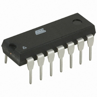
Manufacturer Part Number
ATTINY24A-PU
Description
MCU AVR 2K FLASH 20MHZ 14PDIP
Manufacturer
Atmel
Series
AVR® ATtinyr
Specifications of ATTINY24A-PU
Core Processor
AVR
Core Size
8-Bit
Speed
20MHz
Connectivity
USI
Peripherals
Brown-out Detect/Reset, POR, PWM, Temp Sensor, WDT
Number Of I /o
12
Program Memory Size
2KB (1K x 16)
Program Memory Type
FLASH
Eeprom Size
128 x 8
Ram Size
128 x 8
Voltage - Supply (vcc/vdd)
1.8 V ~ 5.5 V
Data Converters
A/D 8x10b
Oscillator Type
Internal
Operating Temperature
-40°C ~ 85°C
Package / Case
14-DIP (0.300", 7.62mm)
Processor Series
ATTINY2x
Core
AVR8
Data Bus Width
8 bit
Data Ram Size
128 B
Interface Type
SPI, USI
Maximum Clock Frequency
20 MHz
Number Of Programmable I/os
12
Number Of Timers
2
Maximum Operating Temperature
+ 85 C
Mounting Style
Through Hole
3rd Party Development Tools
EWAVR, EWAVR-BL
Development Tools By Supplier
ATAVRDRAGON, ATSTK500, ATSTK600, ATAVRISP2, ATAVRONEKIT
Minimum Operating Temperature
- 40 C
On-chip Adc
10 bit, 20 Channel
Data Rom Size
128 B
A/d Bit Size
10 bit
A/d Channels Available
20
Height
5.33 mm
Length
19.68 mm
Supply Voltage (max)
5.5 V
Supply Voltage (min)
1.8 V
Width
7.11 mm
For Use With
ATSTK505 - ADAPTER KIT FOR 14PIN AVR MCU
Lead Free Status / RoHS Status
Lead free / RoHS Compliant


11.9
11.9.1
8183C–AVR–03/11
Register Description
TCCR0A – Timer/Counter Control Register A
• Bits 7:6 – COM0A[1:0]: Compare Match Output A Mode
These bits control the Output Compare pin (OC0A) behavior. If one or both of the COM0A[1:0]
bits are set, the OC0A output overrides the normal port functionality of the I/O pin it is connected
to. However, note that the Data Direction Register (DDR) bit corresponding to the OC0A pin
must be set in order to enable the output driver.
When OC0A is connected to the pin, the function of the COM0A[1:0] bits depends on the
WGM0[2:0] bit setting.
bits are set to a normal or CTC mode (non-PWM).
Table 11-2.
Table 11-3
Table 11-3.
Note:
Bit
0x30 (0x50)
Read/Write
Initial Value
COM0A1
COM0A1
0
0
1
1
0
0
1
1
1. A special case occurs when OCR0A equals TOP and COM0A1 is set. In this case, the Com-
shows COM0A[1:0] bit functionality when WGM0[1:0] bits are set to fast PWM mode.
pare Match is ignored, but the set or clear is done at BOTTOM. See
page 74
Compare Output Mode, non-PWM Mode
Compare Output Mode, Fast PWM Mode
COM0A1
R/W
COM0A0
COM0A0
7
0
for more details.
0
1
0
1
0
1
0
1
Table 11-2
COM0A0
R/W
6
0
Description
Normal port operation, OC0A disconnected
WGM02 = 0: Normal Port Operation, OC0A Disconnected
WGM02 = 1: Toggle OC0A on Compare Match
Clear OC0A on Compare Match
Set OC0A at BOTTOM (non-inverting mode)
Set OC0A on Compare Match
Clear OC0A at BOTTOM (inverting mode)
Description
Normal port operation, OC0A disconnected.
Toggle OC0A on Compare Match
Clear OC0A on Compare Match
Set OC0A on Compare Match
COM0B1
shows the COM0A[1:0] bit functionality when the WGM0[2:0]
R/W
5
0
COM0B0
R/W
4
0
3
R
0
–
(1)
ATtiny24A/44A/84A
R
2
–
0
WGM01
R/W
1
0
“Fast PWM Mode” on
WGM00
R/W
0
0
TCCR0A
79
Related parts for ATTINY24A-PU
Image
Part Number
Description
Manufacturer
Datasheet
Request
R

Part Number:
Description:
Manufacturer:
Atmel Corporation
Datasheet:
Part Number:
Description:
Manufacturer:
Atmel Corporation
Datasheet:

Part Number:
Description:
IC MCU AVR 2K FLASH 20MHZ 20-QFN
Manufacturer:
Atmel
Datasheet:

Part Number:
Description:
IC MCU AVR 2K FLASH 20MHZ 14SOIC
Manufacturer:
Atmel
Datasheet:

Part Number:
Description:
MCU AVR 2K FLASH 15MHZ 20-QFN
Manufacturer:
Atmel
Datasheet:

Part Number:
Description:
IC MCU AVR 2K FLASH 20MHZ 14-DIP
Manufacturer:
Atmel
Datasheet:

Part Number:
Description:
MCU AVR 2KB FLASH 20MHZ 14SOIC
Manufacturer:
Atmel
Datasheet:
Part Number:
Description:
MCU AVR 2KB FLASH 20MHZ 20QFN
Manufacturer:
Atmel
Datasheet:
Part Number:
Description:
MCU AVR 2K FLASH 15MHZ 14-SOIC
Manufacturer:
Atmel
Datasheet:

Part Number:
Description:
DEV KIT FOR AVR/AVR32
Manufacturer:
Atmel
Datasheet:
Part Number:
Description:
INTERVAL AND WIPE/WASH WIPER CONTROL IC WITH DELAY
Manufacturer:
ATMEL Corporation
Datasheet:
Part Number:
Description:
Low-Voltage Voice-Switched IC for Hands-Free Operation
Manufacturer:
ATMEL Corporation
Datasheet: