ATTINY24A-PU Atmel, ATTINY24A-PU Datasheet - Page 43
ATTINY24A-PU
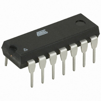
Manufacturer Part Number
ATTINY24A-PU
Description
MCU AVR 2K FLASH 20MHZ 14PDIP
Manufacturer
Atmel
Series
AVR® ATtinyr
Specifications of ATTINY24A-PU
Core Processor
AVR
Core Size
8-Bit
Speed
20MHz
Connectivity
USI
Peripherals
Brown-out Detect/Reset, POR, PWM, Temp Sensor, WDT
Number Of I /o
12
Program Memory Size
2KB (1K x 16)
Program Memory Type
FLASH
Eeprom Size
128 x 8
Ram Size
128 x 8
Voltage - Supply (vcc/vdd)
1.8 V ~ 5.5 V
Data Converters
A/D 8x10b
Oscillator Type
Internal
Operating Temperature
-40°C ~ 85°C
Package / Case
14-DIP (0.300", 7.62mm)
Processor Series
ATTINY2x
Core
AVR8
Data Bus Width
8 bit
Data Ram Size
128 B
Interface Type
SPI, USI
Maximum Clock Frequency
20 MHz
Number Of Programmable I/os
12
Number Of Timers
2
Maximum Operating Temperature
+ 85 C
Mounting Style
Through Hole
3rd Party Development Tools
EWAVR, EWAVR-BL
Development Tools By Supplier
ATAVRDRAGON, ATSTK500, ATSTK600, ATAVRISP2, ATAVRONEKIT
Minimum Operating Temperature
- 40 C
On-chip Adc
10 bit, 20 Channel
Data Rom Size
128 B
A/d Bit Size
10 bit
A/d Channels Available
20
Height
5.33 mm
Length
19.68 mm
Supply Voltage (max)
5.5 V
Supply Voltage (min)
1.8 V
Width
7.11 mm
For Use With
ATSTK505 - ADAPTER KIT FOR 14PIN AVR MCU
Lead Free Status / RoHS Status
Lead free / RoHS Compliant


8.4.2
8183C–AVR–03/11
Code Example
The following code example shows one assembly and one C function for turning off the WDT.
The example assumes that interrupts are controlled (e.g., by disabling interrupts globally) so that
no interrupts will occur during execution of these functions.
Note:
Assembly Code Example
C Code Example
• Safety Level 2
In this mode, the Watchdog Timer is always enabled, and the WDE bit will always read as
one. A timed sequence is needed when changing the Watchdog Time-out period. To change
the Watchdog Time-out, the following procedure must be followed:
WDT_off:
void WDT_off(void)
{
}
a. In the same operation, write a logical one to WDCE and WDE. Even though the
b. Within the next four clock cycles, in the same operation, write the WDP bits as
wdr
; Clear WDRF in MCUSR
ldi
out
; Write logical one to WDCE and WDE
; Keep old prescaler setting to prevent unintentional Watchdog Reset
in
ori r16, (1<<WDCE)|(1<<WDE)
out WDTCSR, r16
; Turn off WDT
ldi r16, (0<<WDE)
out WDTCSR, r16
ret
_WDR();
/* Clear WDRF in MCUSR */
MCUSR = 0x00
/* Write logical one to WDCE and WDE */
WDTCSR |= (1<<WDCE) | (1<<WDE);
/* Turn off WDT */
WDTCSR = 0x00;
See
WDE always is set, the WDE must be written to one to start the timed sequence
desired, but with the WDCE bit cleared. The value written to the WDE bit is
irrelevant
“Code Examples” on page
r16, WDTCSR
r16, (0<<WDRF)
MCUSR, r16
6.
ATtiny24A/44A/84A
43
Related parts for ATTINY24A-PU
Image
Part Number
Description
Manufacturer
Datasheet
Request
R

Part Number:
Description:
Manufacturer:
Atmel Corporation
Datasheet:
Part Number:
Description:
Manufacturer:
Atmel Corporation
Datasheet:

Part Number:
Description:
IC MCU AVR 2K FLASH 20MHZ 20-QFN
Manufacturer:
Atmel
Datasheet:

Part Number:
Description:
IC MCU AVR 2K FLASH 20MHZ 14SOIC
Manufacturer:
Atmel
Datasheet:

Part Number:
Description:
MCU AVR 2K FLASH 15MHZ 20-QFN
Manufacturer:
Atmel
Datasheet:

Part Number:
Description:
IC MCU AVR 2K FLASH 20MHZ 14-DIP
Manufacturer:
Atmel
Datasheet:

Part Number:
Description:
MCU AVR 2KB FLASH 20MHZ 14SOIC
Manufacturer:
Atmel
Datasheet:
Part Number:
Description:
MCU AVR 2KB FLASH 20MHZ 20QFN
Manufacturer:
Atmel
Datasheet:
Part Number:
Description:
MCU AVR 2K FLASH 15MHZ 14-SOIC
Manufacturer:
Atmel
Datasheet:

Part Number:
Description:
DEV KIT FOR AVR/AVR32
Manufacturer:
Atmel
Datasheet:
Part Number:
Description:
INTERVAL AND WIPE/WASH WIPER CONTROL IC WITH DELAY
Manufacturer:
ATMEL Corporation
Datasheet:
Part Number:
Description:
Low-Voltage Voice-Switched IC for Hands-Free Operation
Manufacturer:
ATMEL Corporation
Datasheet: