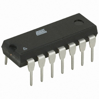
ATTINY24A-PU Atmel, ATTINY24A-PU Datasheet - Page 110

ATTINY24A-PU
Manufacturer Part Number
ATTINY24A-PU
Description
MCU AVR 2K FLASH 20MHZ 14PDIP
Manufacturer
Atmel
Series
AVR® ATtinyr
Specifications of ATTINY24A-PU
Core Processor
AVR
Core Size
8-Bit
Speed
20MHz
Connectivity
USI
Peripherals
Brown-out Detect/Reset, POR, PWM, Temp Sensor, WDT
Number Of I /o
12
Program Memory Size
2KB (1K x 16)
Program Memory Type
FLASH
Eeprom Size
128 x 8
Ram Size
128 x 8
Voltage - Supply (vcc/vdd)
1.8 V ~ 5.5 V
Data Converters
A/D 8x10b
Oscillator Type
Internal
Operating Temperature
-40°C ~ 85°C
Package / Case
14-DIP (0.300", 7.62mm)
Processor Series
ATTINY2x
Core
AVR8
Data Bus Width
8 bit
Data Ram Size
128 B
Interface Type
SPI, USI
Maximum Clock Frequency
20 MHz
Number Of Programmable I/os
12
Number Of Timers
2
Maximum Operating Temperature
+ 85 C
Mounting Style
Through Hole
3rd Party Development Tools
EWAVR, EWAVR-BL
Development Tools By Supplier
ATAVRDRAGON, ATSTK500, ATSTK600, ATAVRISP2, ATAVRONEKIT
Minimum Operating Temperature
- 40 C
On-chip Adc
10 bit, 20 Channel
Data Rom Size
128 B
A/d Bit Size
10 bit
A/d Channels Available
20
Height
5.33 mm
Length
19.68 mm
Supply Voltage (max)
5.5 V
Supply Voltage (min)
1.8 V
Width
7.11 mm
For Use With
ATSTK505 - ADAPTER KIT FOR 14PIN AVR MCU
Lead Free Status / RoHS Status
Lead free / RoHS Compliant
- Current page: 110 of 286
- Download datasheet (10Mb)
12.11.4
12.11.5
12.11.6
110
ATtiny24A/44A/84A
TCNT1H and TCNT1L – Timer/Counter1
OCR1AH and OCR1AL – Output Compare Register 1 A
OCR1BH and OCR1BL – Output Compare Register 1 B
FOC1A/FOC1B bits are implemented as strobes. Therefore it is the value present in the
COM1x[1:0] bits that determine the effect of the forced compare.
A FOC1A/FOC1B strobe will not generate any interrupt nor will it clear the timer in Clear Timer
on Compare match (CTC) mode using OCR1A as TOP.
The FOC1A/FOC1B bits are always read as zero.
• Bits 5:0 – Res: Reserved Bits
These bits are reserved in the ATtiny24A/44A and will always read as zero.
The two Timer/Counter I/O locations (TCNT1H and TCNT1L, combined TCNT1) give direct
access, both for read and for write operations, to the Timer/Counter unit 16-bit counter. To
ensure that both the high and low bytes are read and written simultaneously when the CPU
accesses these registers, the access is performed using an 8-bit temporary high byte register
(TEMP). This temporary register is shared by all the other 16-bit registers. See
Registers” on page
Modifying the counter (TCNT1) while the counter is running introduces a risk of missing a com-
pare match between TCNT1 and one of the OCR1x Registers.
Writing to the TCNT1 Register blocks (removes) the compare match on the following timer clock
for all compare units.
The Output Compare Registers contain a 16-bit value that is continuously compared with the
counter value (TCNT1). A match can be used to generate an Output Compare interrupt, or to
generate a waveform output on the OC1x pin.
The Output Compare Registers are 16-bit in size. To ensure that both the high and low bytes are
written simultaneously when the CPU writes to these registers, the access is performed using an
8-bit temporary high byte register (TEMP). This temporary register is shared by all the other 16-
bit registers. See
Bit
0x2D (0x4D)
0x2C (0x4C)
Read/Write
Initial Value
Bit
0x2B (0x4B)
0x2A (0x4A)
Read/Write
Initial Value
Bit
0x29 (0x49)
0x28 (0x48)
Read/Write
Initial Value
R/W
R/W
R/W
7
0
7
0
7
0
“Accessing 16-bit Registers” on page
103.
R/W
R/W
R/W
6
0
6
0
6
0
R/W
R/W
R/W
5
0
5
0
5
0
R/W
R/W
R/W
4
0
4
0
4
0
OCR1A[15:8]
OCR1B[15:8]
TCNT1[15:8]
OCR1A[7:0]
OCR1B[7:0]
TCNT1[7:0]
R/W
R/W
R/W
3
0
3
0
3
0
103.
R/W
R/W
R/W
2
0
2
0
2
0
R/W
R/W
R/W
1
0
1
0
1
0
“Accessing 16-bit
R/W
R/W
R/W
0
0
0
0
0
0
8183C–AVR–03/11
OCR1AH
OCR1AL
OCR1BH
OCR1BL
TCNT1H
TCNT1L
Related parts for ATTINY24A-PU
Image
Part Number
Description
Manufacturer
Datasheet
Request
R

Part Number:
Description:
Manufacturer:
Atmel Corporation
Datasheet:

Part Number:
Description:
Manufacturer:
Atmel Corporation
Datasheet:

Part Number:
Description:
IC MCU AVR 2K FLASH 20MHZ 20-QFN
Manufacturer:
Atmel
Datasheet:

Part Number:
Description:
IC MCU AVR 2K FLASH 20MHZ 14SOIC
Manufacturer:
Atmel
Datasheet:

Part Number:
Description:
MCU AVR 2K FLASH 15MHZ 20-QFN
Manufacturer:
Atmel
Datasheet:

Part Number:
Description:
IC MCU AVR 2K FLASH 20MHZ 14-DIP
Manufacturer:
Atmel
Datasheet:

Part Number:
Description:
MCU AVR 2KB FLASH 20MHZ 14SOIC
Manufacturer:
Atmel
Datasheet:

Part Number:
Description:
MCU AVR 2KB FLASH 20MHZ 20QFN
Manufacturer:
Atmel
Datasheet:

Part Number:
Description:
MCU AVR 2K FLASH 15MHZ 14-SOIC
Manufacturer:
Atmel
Datasheet:

Part Number:
Description:
DEV KIT FOR AVR/AVR32
Manufacturer:
Atmel
Datasheet:

Part Number:
Description:
INTERVAL AND WIPE/WASH WIPER CONTROL IC WITH DELAY
Manufacturer:
ATMEL Corporation
Datasheet:

Part Number:
Description:
Low-Voltage Voice-Switched IC for Hands-Free Operation
Manufacturer:
ATMEL Corporation
Datasheet:


