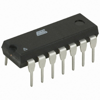
ATTINY24A-PU Atmel, ATTINY24A-PU Datasheet - Page 57

ATTINY24A-PU
Manufacturer Part Number
ATTINY24A-PU
Description
MCU AVR 2K FLASH 20MHZ 14PDIP
Manufacturer
Atmel
Series
AVR® ATtinyr
Specifications of ATTINY24A-PU
Core Processor
AVR
Core Size
8-Bit
Speed
20MHz
Connectivity
USI
Peripherals
Brown-out Detect/Reset, POR, PWM, Temp Sensor, WDT
Number Of I /o
12
Program Memory Size
2KB (1K x 16)
Program Memory Type
FLASH
Eeprom Size
128 x 8
Ram Size
128 x 8
Voltage - Supply (vcc/vdd)
1.8 V ~ 5.5 V
Data Converters
A/D 8x10b
Oscillator Type
Internal
Operating Temperature
-40°C ~ 85°C
Package / Case
14-DIP (0.300", 7.62mm)
Processor Series
ATTINY2x
Core
AVR8
Data Bus Width
8 bit
Data Ram Size
128 B
Interface Type
SPI, USI
Maximum Clock Frequency
20 MHz
Number Of Programmable I/os
12
Number Of Timers
2
Maximum Operating Temperature
+ 85 C
Mounting Style
Through Hole
3rd Party Development Tools
EWAVR, EWAVR-BL
Development Tools By Supplier
ATAVRDRAGON, ATSTK500, ATSTK600, ATAVRISP2, ATAVRONEKIT
Minimum Operating Temperature
- 40 C
On-chip Adc
10 bit, 20 Channel
Data Rom Size
128 B
A/d Bit Size
10 bit
A/d Channels Available
20
Height
5.33 mm
Length
19.68 mm
Supply Voltage (max)
5.5 V
Supply Voltage (min)
1.8 V
Width
7.11 mm
For Use With
ATSTK505 - ADAPTER KIT FOR 14PIN AVR MCU
Lead Free Status / RoHS Status
Lead free / RoHS Compliant
- Current page: 57 of 286
- Download datasheet (10Mb)
10.1.7
8183C–AVR–03/11
Program Examples
important, it is recommended to use an external pull-up or pulldown. Connecting unused pins
directly to V
accidentally configured as an output.
The following code example shows how to set port A pins 0 and 1 high, 2 and 3 low, and define
the port pins from 4 to 5 as input with a pull-up assigned to port pin 4. The resulting pin values
are read back again, but as previously discussed, a nop instruction is included to be able to read
back the value recently assigned to some of the pins.
Note:
Note:
Assembly Code Example
C Code Example
unsigned char i;
...
; Define pull-ups and set outputs high
; Define directions for port pins
ldi
ldi
out
out
; Insert nop for synchronization
nop
; Read port pins
in
...
...
/* Define pull-ups and set outputs high */
/* Define directions for port pins */
PORTA = (1<<PA4)|(1<<PA1)|(1<<PA0);
DDRA = (1<<DDA3)|(1<<DDA2)|(1<<DDA1)|(1<<DDA0);
/* Insert nop for synchronization*/
_NOP();
/* Read port pins */
i = PINA;
...
Two temporary registers are used to minimize the time from pull-ups are set on pins 0, 1 and 4,
until the direction bits are correctly set, defining bit 2 and 3 as low and redefining bits 0 and 1 as
strong high drivers.
See
CC
“Code Examples” on page
r16,(1<<PA4)|(1<<PA1)|(1<<PA0)
r17,(1<<DDA3)|(1<<DDA2)|(1<<DDA1)|(1<<DDA0)
PORTA,r16
DDRA,r17
r16,PINA
or GND is not recommended, since this may cause excessive currents if the pin is
6.
ATtiny24A/44A/84A
57
Related parts for ATTINY24A-PU
Image
Part Number
Description
Manufacturer
Datasheet
Request
R

Part Number:
Description:
Manufacturer:
Atmel Corporation
Datasheet:

Part Number:
Description:
Manufacturer:
Atmel Corporation
Datasheet:

Part Number:
Description:
IC MCU AVR 2K FLASH 20MHZ 20-QFN
Manufacturer:
Atmel
Datasheet:

Part Number:
Description:
IC MCU AVR 2K FLASH 20MHZ 14SOIC
Manufacturer:
Atmel
Datasheet:

Part Number:
Description:
MCU AVR 2K FLASH 15MHZ 20-QFN
Manufacturer:
Atmel
Datasheet:

Part Number:
Description:
IC MCU AVR 2K FLASH 20MHZ 14-DIP
Manufacturer:
Atmel
Datasheet:

Part Number:
Description:
MCU AVR 2KB FLASH 20MHZ 14SOIC
Manufacturer:
Atmel
Datasheet:

Part Number:
Description:
MCU AVR 2KB FLASH 20MHZ 20QFN
Manufacturer:
Atmel
Datasheet:

Part Number:
Description:
MCU AVR 2K FLASH 15MHZ 14-SOIC
Manufacturer:
Atmel
Datasheet:

Part Number:
Description:
DEV KIT FOR AVR/AVR32
Manufacturer:
Atmel
Datasheet:

Part Number:
Description:
INTERVAL AND WIPE/WASH WIPER CONTROL IC WITH DELAY
Manufacturer:
ATMEL Corporation
Datasheet:

Part Number:
Description:
Low-Voltage Voice-Switched IC for Hands-Free Operation
Manufacturer:
ATMEL Corporation
Datasheet:


