ATTINY24A-PU Atmel, ATTINY24A-PU Datasheet - Page 160
ATTINY24A-PU
Manufacturer Part Number
ATTINY24A-PU
Description
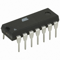
MCU AVR 2K FLASH 20MHZ 14PDIP
Manufacturer
Atmel
Series
AVR® ATtinyr
Specifications of ATTINY24A-PU
Core Processor
AVR
Core Size
8-Bit
Speed
20MHz
Connectivity
USI
Peripherals
Brown-out Detect/Reset, POR, PWM, Temp Sensor, WDT
Number Of I /o
12
Program Memory Size
2KB (1K x 16)
Program Memory Type
FLASH
Eeprom Size
128 x 8
Ram Size
128 x 8
Voltage - Supply (vcc/vdd)
1.8 V ~ 5.5 V
Data Converters
A/D 8x10b
Oscillator Type
Internal
Operating Temperature
-40°C ~ 85°C
Package / Case
14-DIP (0.300", 7.62mm)
Processor Series
ATTINY2x
Core
AVR8
Data Bus Width
8 bit
Data Ram Size
128 B
Interface Type
SPI, USI
Maximum Clock Frequency
20 MHz
Number Of Programmable I/os
12
Number Of Timers
2
Maximum Operating Temperature
+ 85 C
Mounting Style
Through Hole
3rd Party Development Tools
EWAVR, EWAVR-BL
Development Tools By Supplier
ATAVRDRAGON, ATSTK500, ATSTK600, ATAVRISP2, ATAVRONEKIT
Minimum Operating Temperature
- 40 C
On-chip Adc
10 bit, 20 Channel
Data Rom Size
128 B
A/d Bit Size
10 bit
A/d Channels Available
20
Height
5.33 mm
Length
19.68 mm
Supply Voltage (max)
5.5 V
Supply Voltage (min)
1.8 V
Width
7.11 mm
For Use With
ATSTK505 - ADAPTER KIT FOR 14PIN AVR MCU
Lead Free Status / RoHS Status
Lead free / RoHS Compliant


19.2.1
19.3
160
Device Signature Imprint Table
ATtiny24A/44A/84A
Latching of Fuses
Table 19-5.
Notes:
Note that fuse bits are locked if Lock Bit 1 (LB1) is programmed. Fuse bits should be pro-
grammed before lock bits. The status of fuse bits is not affected by chip erase.
Fuse bits can also be read by device firmware. See section
Data from Software” on page
Fuse values are latched when the device enters programming mode and changes to fuse values
have no effect until the part leaves programming mode. This does not apply to the EESAVE
Fuse which will take effect once it is programmed. Fuses are also latched on power-up.
The device signature imprint table is a dedicated memory area used for storing miscellaneous
device information, such as the device signature and oscillator calibaration data. Most of this
memory segment is reserved for internal use, as outlined in
Table 19-6.
Notes:
Fuse Low Byte
CKDIV8
CKOUT
SUT1
SUT0
CKSEL3
CKSEL2
CKSEL1
CKSEL0
Address
0x00
0x01
0x02
0x03
0x04
0x05 ... 0x2A
(3)
(3)
1. See
2. Allows system clock to be output on pin. See
3. The default value results in maximum start-up time for the default clock source. See
4. The default setting results in internal RC Oscillator @ 8.0 MHz. See
1. See section “Signature Bytes” for more information.
2. See section “Calibration Byte” for more information.
(2)
(1)
(4)
(4)
(4)
(4)
on page 27
details.
Fuse Low Byte
Contents of Device Signature Imprint Table.
“System Clock Prescaler” on page 30
High Byte
Signature byte 0
Calibration data for internal oscillator
Signature byte 1
Reserved for internal use
Signature byte 2
Reserved for internal use
for details.
Bit No
154.
7
6
5
4
3
2
1
0
(1)
(1)
(1)
Description
Divide clock by 8
Clock Output Enable
Select start-up time
Select start-up time
Select Clock source
Select Clock source
Select Clock source
Select Clock source
for details.
(2)
“Clock Output Buffer” on page 30
“Reading Lock, Fuse and Signature
Table
19-6.
0 (programmed)
Default Value
0 (programmed)
1 (unprogrammed)
1 (unprogrammed)
0 (programmed)
0 (programmed)
1 (unprogrammed)
0 (programmed)
Table 6-4 on page 27
8183C–AVR–03/11
for details.
Table 6-5
for
Related parts for ATTINY24A-PU
Image
Part Number
Description
Manufacturer
Datasheet
Request
R

Part Number:
Description:
Manufacturer:
Atmel Corporation
Datasheet:
Part Number:
Description:
Manufacturer:
Atmel Corporation
Datasheet:

Part Number:
Description:
IC MCU AVR 2K FLASH 20MHZ 20-QFN
Manufacturer:
Atmel
Datasheet:

Part Number:
Description:
IC MCU AVR 2K FLASH 20MHZ 14SOIC
Manufacturer:
Atmel
Datasheet:

Part Number:
Description:
MCU AVR 2K FLASH 15MHZ 20-QFN
Manufacturer:
Atmel
Datasheet:

Part Number:
Description:
IC MCU AVR 2K FLASH 20MHZ 14-DIP
Manufacturer:
Atmel
Datasheet:

Part Number:
Description:
MCU AVR 2KB FLASH 20MHZ 14SOIC
Manufacturer:
Atmel
Datasheet:
Part Number:
Description:
MCU AVR 2KB FLASH 20MHZ 20QFN
Manufacturer:
Atmel
Datasheet:
Part Number:
Description:
MCU AVR 2K FLASH 15MHZ 14-SOIC
Manufacturer:
Atmel
Datasheet:

Part Number:
Description:
DEV KIT FOR AVR/AVR32
Manufacturer:
Atmel
Datasheet:
Part Number:
Description:
INTERVAL AND WIPE/WASH WIPER CONTROL IC WITH DELAY
Manufacturer:
ATMEL Corporation
Datasheet:
Part Number:
Description:
Low-Voltage Voice-Switched IC for Hands-Free Operation
Manufacturer:
ATMEL Corporation
Datasheet: