ATTINY24A-PU Atmel, ATTINY24A-PU Datasheet - Page 32
ATTINY24A-PU
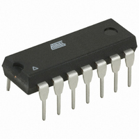
Manufacturer Part Number
ATTINY24A-PU
Description
MCU AVR 2K FLASH 20MHZ 14PDIP
Manufacturer
Atmel
Series
AVR® ATtinyr
Specifications of ATTINY24A-PU
Core Processor
AVR
Core Size
8-Bit
Speed
20MHz
Connectivity
USI
Peripherals
Brown-out Detect/Reset, POR, PWM, Temp Sensor, WDT
Number Of I /o
12
Program Memory Size
2KB (1K x 16)
Program Memory Type
FLASH
Eeprom Size
128 x 8
Ram Size
128 x 8
Voltage - Supply (vcc/vdd)
1.8 V ~ 5.5 V
Data Converters
A/D 8x10b
Oscillator Type
Internal
Operating Temperature
-40°C ~ 85°C
Package / Case
14-DIP (0.300", 7.62mm)
Processor Series
ATTINY2x
Core
AVR8
Data Bus Width
8 bit
Data Ram Size
128 B
Interface Type
SPI, USI
Maximum Clock Frequency
20 MHz
Number Of Programmable I/os
12
Number Of Timers
2
Maximum Operating Temperature
+ 85 C
Mounting Style
Through Hole
3rd Party Development Tools
EWAVR, EWAVR-BL
Development Tools By Supplier
ATAVRDRAGON, ATSTK500, ATSTK600, ATAVRISP2, ATAVRONEKIT
Minimum Operating Temperature
- 40 C
On-chip Adc
10 bit, 20 Channel
Data Rom Size
128 B
A/d Bit Size
10 bit
A/d Channels Available
20
Height
5.33 mm
Length
19.68 mm
Supply Voltage (max)
5.5 V
Supply Voltage (min)
1.8 V
Width
7.11 mm
For Use With
ATSTK505 - ADAPTER KIT FOR 14PIN AVR MCU
Lead Free Status / RoHS Status
Lead free / RoHS Compliant


32
ATtiny24A/44A/84A
• Bits 3:0 – CLKPS[3:0]: Clock Prescaler Select Bits 3 - 0
These bits define the division factor between the selected clock source and the internal system
clock. These bits can be written run-time to vary the clock frequency to suit the application
requirements. As the divider divides the master clock input to the MCU, the speed of all synchro-
nous peripherals is reduced when a division factor is used. The division factors are given in
Table 6-11 on page
To avoid unintentional changes of clock frequency, a special write procedure must be followed
to change the CLKPS bits:
Interrupts must be disabled when changing prescaler setting to make sure the write procedure is
not interrupted.
The CKDIV8 Fuse determines the initial value of the CLKPS bits. If CKDIV8 is unprogrammed,
the CLKPS bits will be reset to “0000”. If CKDIV8 is programmed, CLKPS bits are reset to
“0011”, giving a division factor of eight at start up. This feature should be used if the selected
clock source has a higher frequency than the maximum frequency of the device at the present
operating conditions. Note that any value can be written to the CLKPS bits regardless of the
CKDIV8 Fuse setting. The Application software must ensure that a sufficient division factor is
chosen if the selcted clock source has a higher frequency than the maximum frequency of the
device at the present operating conditions. The device is shipped with the CKDIV8 Fuse
programmed.
Table 6-11.
1. Write the Clock Prescaler Change Enable (CLKPCE) bit to one and all other bits in
2. Within four cycles, write the desired value to CLKPS while writing a zero to CLKPCE.
CLKPS3
CLKPR to zero.
0
0
0
0
0
0
0
0
1
1
1
1
1
1
1
1
Clock Prescaler Select
CLKPS2
32.
0
0
0
0
1
1
1
1
0
0
0
0
1
1
1
1
CLKPS1
0
0
1
1
0
0
1
1
0
0
1
1
0
0
1
1
CLKPS0
0
1
0
1
0
1
0
1
0
1
0
1
0
1
0
1
Clock Division Factor
Reserved
Reserved
Reserved
Reserved
Reserved
Reserved
Reserved
128
256
16
32
64
1
2
4
8
8183C–AVR–03/11
Related parts for ATTINY24A-PU
Image
Part Number
Description
Manufacturer
Datasheet
Request
R

Part Number:
Description:
Manufacturer:
Atmel Corporation
Datasheet:
Part Number:
Description:
Manufacturer:
Atmel Corporation
Datasheet:

Part Number:
Description:
IC MCU AVR 2K FLASH 20MHZ 20-QFN
Manufacturer:
Atmel
Datasheet:

Part Number:
Description:
IC MCU AVR 2K FLASH 20MHZ 14SOIC
Manufacturer:
Atmel
Datasheet:

Part Number:
Description:
MCU AVR 2K FLASH 15MHZ 20-QFN
Manufacturer:
Atmel
Datasheet:

Part Number:
Description:
IC MCU AVR 2K FLASH 20MHZ 14-DIP
Manufacturer:
Atmel
Datasheet:

Part Number:
Description:
MCU AVR 2KB FLASH 20MHZ 14SOIC
Manufacturer:
Atmel
Datasheet:
Part Number:
Description:
MCU AVR 2KB FLASH 20MHZ 20QFN
Manufacturer:
Atmel
Datasheet:
Part Number:
Description:
MCU AVR 2K FLASH 15MHZ 14-SOIC
Manufacturer:
Atmel
Datasheet:

Part Number:
Description:
DEV KIT FOR AVR/AVR32
Manufacturer:
Atmel
Datasheet:
Part Number:
Description:
INTERVAL AND WIPE/WASH WIPER CONTROL IC WITH DELAY
Manufacturer:
ATMEL Corporation
Datasheet:
Part Number:
Description:
Low-Voltage Voice-Switched IC for Hands-Free Operation
Manufacturer:
ATMEL Corporation
Datasheet: