ATTINY24A-PU Atmel, ATTINY24A-PU Datasheet - Page 114
ATTINY24A-PU
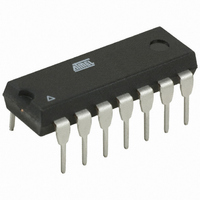
Manufacturer Part Number
ATTINY24A-PU
Description
MCU AVR 2K FLASH 20MHZ 14PDIP
Manufacturer
Atmel
Series
AVR® ATtinyr
Specifications of ATTINY24A-PU
Core Processor
AVR
Core Size
8-Bit
Speed
20MHz
Connectivity
USI
Peripherals
Brown-out Detect/Reset, POR, PWM, Temp Sensor, WDT
Number Of I /o
12
Program Memory Size
2KB (1K x 16)
Program Memory Type
FLASH
Eeprom Size
128 x 8
Ram Size
128 x 8
Voltage - Supply (vcc/vdd)
1.8 V ~ 5.5 V
Data Converters
A/D 8x10b
Oscillator Type
Internal
Operating Temperature
-40°C ~ 85°C
Package / Case
14-DIP (0.300", 7.62mm)
Processor Series
ATTINY2x
Core
AVR8
Data Bus Width
8 bit
Data Ram Size
128 B
Interface Type
SPI, USI
Maximum Clock Frequency
20 MHz
Number Of Programmable I/os
12
Number Of Timers
2
Maximum Operating Temperature
+ 85 C
Mounting Style
Through Hole
3rd Party Development Tools
EWAVR, EWAVR-BL
Development Tools By Supplier
ATAVRDRAGON, ATSTK500, ATSTK600, ATAVRISP2, ATAVRONEKIT
Minimum Operating Temperature
- 40 C
On-chip Adc
10 bit, 20 Channel
Data Rom Size
128 B
A/d Bit Size
10 bit
A/d Channels Available
20
Height
5.33 mm
Length
19.68 mm
Supply Voltage (max)
5.5 V
Supply Voltage (min)
1.8 V
Width
7.11 mm
For Use With
ATSTK505 - ADAPTER KIT FOR 14PIN AVR MCU
Lead Free Status / RoHS Status
Lead free / RoHS Compliant


13.3
13.3.1
114
Register Description
ATtiny24A/44A/84A
GTCCR – General Timer/Counter Control Register
Enabling and disabling of the clock input must be done when Tn has been stable for at least one
system clock cycle, otherwise it is a risk that a false Timer/Counter clock pulse is generated.
Each half period of the external clock applied must be longer than one system clock cycle to
ensure correct sampling. The external clock must be guaranteed to have less than half the sys-
tem clock frequency (f
sampling, the maximum frequency of an external clock it can detect is half the sampling fre-
quency (Nyquist sampling theorem). However, due to variation of the system clock frequency
and duty cycle caused by Oscillator source (crystal, resonator, and capacitors) tolerances, it is
recommended that maximum frequency of an external clock source is less than f
An external clock source can not be prescaled.
Figure 13-2.
Note:
• Bit 7 – TSM: Timer/Counter Synchronization Mode
Writing the TSM bit to one activates the Timer/Counter Synchronization mode. In this mode, the
value that is written to the PSR10 bit is kept, hence keeping the Prescaler Reset signal asserted.
This ensures that the Timer/Counter is halted and can be configured without the risk of advanc-
PSR10
clk
Bit
0x23 (0x43)
Read/Write
Initial Value
T0
I/O
1. The synchronization logic on the input pins (
Synchronization
TSM
R/W
Prescaler for Timer/Counter0
7
0
ExtClk
R
6
–
0
< f
Clear
clk_I/O
/2) given a 50/50% duty cycle. Since the edge detector uses
R
5
–
0
R
4
–
0
T0)
is shown in
R
3
–
0
R
2
–
0
Figure 13-1 on page
clk
T0
R
1
–
0
PSR10
clk_I/O
R/W
0
0
8183C–AVR–03/11
113.
/2.5.
GTCCR
Related parts for ATTINY24A-PU
Image
Part Number
Description
Manufacturer
Datasheet
Request
R

Part Number:
Description:
Manufacturer:
Atmel Corporation
Datasheet:
Part Number:
Description:
Manufacturer:
Atmel Corporation
Datasheet:

Part Number:
Description:
IC MCU AVR 2K FLASH 20MHZ 20-QFN
Manufacturer:
Atmel
Datasheet:

Part Number:
Description:
IC MCU AVR 2K FLASH 20MHZ 14SOIC
Manufacturer:
Atmel
Datasheet:

Part Number:
Description:
MCU AVR 2K FLASH 15MHZ 20-QFN
Manufacturer:
Atmel
Datasheet:

Part Number:
Description:
IC MCU AVR 2K FLASH 20MHZ 14-DIP
Manufacturer:
Atmel
Datasheet:

Part Number:
Description:
MCU AVR 2KB FLASH 20MHZ 14SOIC
Manufacturer:
Atmel
Datasheet:
Part Number:
Description:
MCU AVR 2KB FLASH 20MHZ 20QFN
Manufacturer:
Atmel
Datasheet:
Part Number:
Description:
MCU AVR 2K FLASH 15MHZ 14-SOIC
Manufacturer:
Atmel
Datasheet:

Part Number:
Description:
DEV KIT FOR AVR/AVR32
Manufacturer:
Atmel
Datasheet:
Part Number:
Description:
INTERVAL AND WIPE/WASH WIPER CONTROL IC WITH DELAY
Manufacturer:
ATMEL Corporation
Datasheet:
Part Number:
Description:
Low-Voltage Voice-Switched IC for Hands-Free Operation
Manufacturer:
ATMEL Corporation
Datasheet: