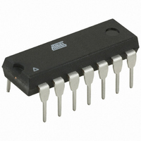
ATTINY24A-PU Atmel, ATTINY24A-PU Datasheet - Page 166

ATTINY24A-PU
Manufacturer Part Number
ATTINY24A-PU
Description
MCU AVR 2K FLASH 20MHZ 14PDIP
Manufacturer
Atmel
Series
AVR® ATtinyr
Specifications of ATTINY24A-PU
Core Processor
AVR
Core Size
8-Bit
Speed
20MHz
Connectivity
USI
Peripherals
Brown-out Detect/Reset, POR, PWM, Temp Sensor, WDT
Number Of I /o
12
Program Memory Size
2KB (1K x 16)
Program Memory Type
FLASH
Eeprom Size
128 x 8
Ram Size
128 x 8
Voltage - Supply (vcc/vdd)
1.8 V ~ 5.5 V
Data Converters
A/D 8x10b
Oscillator Type
Internal
Operating Temperature
-40°C ~ 85°C
Package / Case
14-DIP (0.300", 7.62mm)
Processor Series
ATTINY2x
Core
AVR8
Data Bus Width
8 bit
Data Ram Size
128 B
Interface Type
SPI, USI
Maximum Clock Frequency
20 MHz
Number Of Programmable I/os
12
Number Of Timers
2
Maximum Operating Temperature
+ 85 C
Mounting Style
Through Hole
3rd Party Development Tools
EWAVR, EWAVR-BL
Development Tools By Supplier
ATAVRDRAGON, ATSTK500, ATSTK600, ATAVRISP2, ATAVRONEKIT
Minimum Operating Temperature
- 40 C
On-chip Adc
10 bit, 20 Channel
Data Rom Size
128 B
A/d Bit Size
10 bit
A/d Channels Available
20
Height
5.33 mm
Length
19.68 mm
Supply Voltage (max)
5.5 V
Supply Voltage (min)
1.8 V
Width
7.11 mm
For Use With
ATSTK505 - ADAPTER KIT FOR 14PIN AVR MCU
Lead Free Status / RoHS Status
Lead free / RoHS Compliant
- Current page: 166 of 286
- Download datasheet (10Mb)
19.6
19.7
166
High-voltage Serial Programming
High-Voltage Serial Programming Algorithm
ATtiny24A/44A/84A
After data is loaded to the page buffer, program the EEPROM page, see
165.
This section describes how to program and verify Flash Program memory, EEPROM Data mem-
ory, Lock bits and Fuse bits in the ATtiny24A/44A/84A.
Figure 19-3.
Table 19-13. Pin Name Mapping
The minimum period for the Serial Clock Input (SCI) during High-voltage Serial Programming is
220 ns.
Table 19-14. Pin Values Used to Enter Programming Mode
To program and verify the ATtiny24A/44A/84A in the High-voltage Serial Programming mode,
the following sequence is recommended (See instruction formats in
Signal Name in High-voltage
Serial Programming Mode
SDI
SII
SDO
SCI
Pin
PA0
PA1
PA2
High-voltage Serial Programming
SCI
+11.5 - 12.5V
Symbol
Prog_enable[0]
Prog_enable[1]
Prog_enable[2]
PB3
PB0
PA2:0
GND
Pin Name
PA6
PA5
PA4
PB0
(RESET)
I/O
O
I
I
I
VCC
PA4
PA5
PA6
Function
Serial Data Input
Serial Instruction Input
Serial Data Output
Serial Clock Input (min. 220ns period)
+4.5 - 5.5V
Table 19-16 on page
SDO
SII
SDI
Figure 19-2 on page
Value
8183C–AVR–03/11
0
0
0
170):
Related parts for ATTINY24A-PU
Image
Part Number
Description
Manufacturer
Datasheet
Request
R

Part Number:
Description:
Manufacturer:
Atmel Corporation
Datasheet:

Part Number:
Description:
Manufacturer:
Atmel Corporation
Datasheet:

Part Number:
Description:
IC MCU AVR 2K FLASH 20MHZ 20-QFN
Manufacturer:
Atmel
Datasheet:

Part Number:
Description:
IC MCU AVR 2K FLASH 20MHZ 14SOIC
Manufacturer:
Atmel
Datasheet:

Part Number:
Description:
MCU AVR 2K FLASH 15MHZ 20-QFN
Manufacturer:
Atmel
Datasheet:

Part Number:
Description:
IC MCU AVR 2K FLASH 20MHZ 14-DIP
Manufacturer:
Atmel
Datasheet:

Part Number:
Description:
MCU AVR 2KB FLASH 20MHZ 14SOIC
Manufacturer:
Atmel
Datasheet:

Part Number:
Description:
MCU AVR 2KB FLASH 20MHZ 20QFN
Manufacturer:
Atmel
Datasheet:

Part Number:
Description:
MCU AVR 2K FLASH 15MHZ 14-SOIC
Manufacturer:
Atmel
Datasheet:

Part Number:
Description:
DEV KIT FOR AVR/AVR32
Manufacturer:
Atmel
Datasheet:

Part Number:
Description:
INTERVAL AND WIPE/WASH WIPER CONTROL IC WITH DELAY
Manufacturer:
ATMEL Corporation
Datasheet:

Part Number:
Description:
Low-Voltage Voice-Switched IC for Hands-Free Operation
Manufacturer:
ATMEL Corporation
Datasheet:


