ATTINY24A-PU Atmel, ATTINY24A-PU Datasheet - Page 174
ATTINY24A-PU
Manufacturer Part Number
ATTINY24A-PU
Description
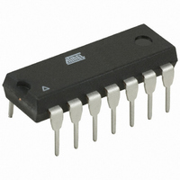
MCU AVR 2K FLASH 20MHZ 14PDIP
Manufacturer
Atmel
Series
AVR® ATtinyr
Specifications of ATTINY24A-PU
Core Processor
AVR
Core Size
8-Bit
Speed
20MHz
Connectivity
USI
Peripherals
Brown-out Detect/Reset, POR, PWM, Temp Sensor, WDT
Number Of I /o
12
Program Memory Size
2KB (1K x 16)
Program Memory Type
FLASH
Eeprom Size
128 x 8
Ram Size
128 x 8
Voltage - Supply (vcc/vdd)
1.8 V ~ 5.5 V
Data Converters
A/D 8x10b
Oscillator Type
Internal
Operating Temperature
-40°C ~ 85°C
Package / Case
14-DIP (0.300", 7.62mm)
Processor Series
ATTINY2x
Core
AVR8
Data Bus Width
8 bit
Data Ram Size
128 B
Interface Type
SPI, USI
Maximum Clock Frequency
20 MHz
Number Of Programmable I/os
12
Number Of Timers
2
Maximum Operating Temperature
+ 85 C
Mounting Style
Through Hole
3rd Party Development Tools
EWAVR, EWAVR-BL
Development Tools By Supplier
ATAVRDRAGON, ATSTK500, ATSTK600, ATAVRISP2, ATAVRONEKIT
Minimum Operating Temperature
- 40 C
On-chip Adc
10 bit, 20 Channel
Data Rom Size
128 B
A/d Bit Size
10 bit
A/d Channels Available
20
Height
5.33 mm
Length
19.68 mm
Supply Voltage (max)
5.5 V
Supply Voltage (min)
1.8 V
Width
7.11 mm
For Use With
ATSTK505 - ADAPTER KIT FOR 14PIN AVR MCU
Lead Free Status / RoHS Status
Lead free / RoHS Compliant


Table 20-1.
Notes:
20.3
174
Symbol
I
CC
1. Typical values at 25°C.
2. “Min” means the lowest value where the pin is guaranteed to be read as high.
3. “Max” means the highest value where the pin is guaranteed to be read as low.
4. Not tested in production.
5. Although each I/O port can sink more than the test conditions (10 mA at V
6. Although each I/O port can source more than the test conditions (10 mA at V
7. The RESET pin must tolerate high voltages when entering and operating in programming modes and, as a consequence,
8. These are test limits, which account for leakage currents of the test environment. Actual device leakage currents are lower.
9. Values are with external clock using methods described in
10. BOD Disabled.
Speed
ATtiny24A/44A/84A
conditions (non-transient), the sum of all I
may exceed the related specification. Pins are not guaranteed to sink current greater than the listed test condition.
conditions (non-transient), the sum of all I
may exceed the related specification. Pins are not guaranteed to source current greater than the listed test condition.
has a weak drive strength as compared to regular I/O pins. See
(starting on
enabled (PRR = 0xFF) and there is no I/O drive.
Parameter
Supply Current,
Active Mode
Supply Current,
Idle Mode
Supply Current,
Power-Down Mode
DC Characteristics. T
(9)
page
(9)
The maximum operating frequency of the device depends on V
relationship between maximum frequency and V
Figure 20-1.
226).
(10)
A
= -40°C to +85°C (Continued)
20 MHz
Condition
f = 1 MHz, V
f = 4 MHz, V
f = 8 MHz, V
f = 1 MHz, V
f = 4 MHz, V
f = 8 MHz, V
WDT enabled, V
WDT disabled, V
4 MHz
Maximum Frequency vs. V
OL
OH
1.8V
(for all ports) should not exceed 60 mA. If I
(for all ports) should not exceed 60 mA. If I
CC
CC
CC
CC
CC
CC
= 2V
= 3V
= 5V
= 2V
= 3V
= 5V
CC
CC
= 3V
= 3V
“Minimizing Power Consumption” on page
Figure
CC
Min
21-87,
CC
is linear in the region 1.8V < V
CC
CC
= 5V, 5 mA at V
Figure
= 5V, 5 mA at V
Typ
0.25
0.04
0.25
0.13
1.2
4.4
1.3
4.5V
21-88,
4
(1)
OL
OH
CC.
exceeds the test conditions, V
exceeds the test condition, V
As shown in
Figure
CC
CC
= 3V) under steady state
= 3V) under steady state
21-89, and
5.5V
Max
35. Power Reduction is
0.5
0.2
0.6
10
2
2
7
2
Figure
CC
8183C–AVR–03/11
Figure 21-90
< 4.5V.
20-1, the
Units
mA
mA
mA
mA
mA
mA
µA
µA
OH
OL
Related parts for ATTINY24A-PU
Image
Part Number
Description
Manufacturer
Datasheet
Request
R

Part Number:
Description:
Manufacturer:
Atmel Corporation
Datasheet:
Part Number:
Description:
Manufacturer:
Atmel Corporation
Datasheet:

Part Number:
Description:
IC MCU AVR 2K FLASH 20MHZ 20-QFN
Manufacturer:
Atmel
Datasheet:

Part Number:
Description:
IC MCU AVR 2K FLASH 20MHZ 14SOIC
Manufacturer:
Atmel
Datasheet:

Part Number:
Description:
MCU AVR 2K FLASH 15MHZ 20-QFN
Manufacturer:
Atmel
Datasheet:

Part Number:
Description:
IC MCU AVR 2K FLASH 20MHZ 14-DIP
Manufacturer:
Atmel
Datasheet:

Part Number:
Description:
MCU AVR 2KB FLASH 20MHZ 14SOIC
Manufacturer:
Atmel
Datasheet:
Part Number:
Description:
MCU AVR 2KB FLASH 20MHZ 20QFN
Manufacturer:
Atmel
Datasheet:
Part Number:
Description:
MCU AVR 2K FLASH 15MHZ 14-SOIC
Manufacturer:
Atmel
Datasheet:

Part Number:
Description:
DEV KIT FOR AVR/AVR32
Manufacturer:
Atmel
Datasheet:
Part Number:
Description:
INTERVAL AND WIPE/WASH WIPER CONTROL IC WITH DELAY
Manufacturer:
ATMEL Corporation
Datasheet:
Part Number:
Description:
Low-Voltage Voice-Switched IC for Hands-Free Operation
Manufacturer:
ATMEL Corporation
Datasheet: