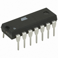
ATTINY24A-PU Atmel, ATTINY24A-PU Datasheet - Page 182

ATTINY24A-PU
Manufacturer Part Number
ATTINY24A-PU
Description
MCU AVR 2K FLASH 20MHZ 14PDIP
Manufacturer
Atmel
Series
AVR® ATtinyr
Specifications of ATTINY24A-PU
Core Processor
AVR
Core Size
8-Bit
Speed
20MHz
Connectivity
USI
Peripherals
Brown-out Detect/Reset, POR, PWM, Temp Sensor, WDT
Number Of I /o
12
Program Memory Size
2KB (1K x 16)
Program Memory Type
FLASH
Eeprom Size
128 x 8
Ram Size
128 x 8
Voltage - Supply (vcc/vdd)
1.8 V ~ 5.5 V
Data Converters
A/D 8x10b
Oscillator Type
Internal
Operating Temperature
-40°C ~ 85°C
Package / Case
14-DIP (0.300", 7.62mm)
Processor Series
ATTINY2x
Core
AVR8
Data Bus Width
8 bit
Data Ram Size
128 B
Interface Type
SPI, USI
Maximum Clock Frequency
20 MHz
Number Of Programmable I/os
12
Number Of Timers
2
Maximum Operating Temperature
+ 85 C
Mounting Style
Through Hole
3rd Party Development Tools
EWAVR, EWAVR-BL
Development Tools By Supplier
ATAVRDRAGON, ATSTK500, ATSTK600, ATAVRISP2, ATAVRONEKIT
Minimum Operating Temperature
- 40 C
On-chip Adc
10 bit, 20 Channel
Data Rom Size
128 B
A/d Bit Size
10 bit
A/d Channels Available
20
Height
5.33 mm
Length
19.68 mm
Supply Voltage (max)
5.5 V
Supply Voltage (min)
1.8 V
Width
7.11 mm
For Use With
ATSTK505 - ADAPTER KIT FOR 14PIN AVR MCU
Lead Free Status / RoHS Status
Lead free / RoHS Compliant
- Current page: 182 of 286
- Download datasheet (10Mb)
21. Typical Characteristics
21.1
182
Supply Current of I/O Modules
ATtiny24A/44A/84A
The data contained in this section is largely based on simulations and characterization of similar
devices in the same process and design methods. Thus, the data should be treated as indica-
tions of how the part will behave.
The following charts show typical behavior. These figures are not tested during manufacturing.
During characterisation devices are operated at frequencies higher than test limits but they are
not guaranteed to function properly at frequencies higher than the ordering code indicates.
All current consumption measurements are performed with all I/O pins configured as inputs and
with internal pull-ups enabled. Current consumption is a function of several factors such as oper-
ating voltage, operating frequency, loading of I/O pins, switching rate of I/O pins, code executed
and ambient temperature. The dominating factors are operating voltage and frequency.
A sine wave generator with rail-to-rail output is used as clock source but current consumption in
Power-Down mode is independent of clock selection. The difference between current consump-
tion in Power-Down mode with Watchdog Timer enabled and Power-Down mode with Watchdog
Timer disabled represents the differential current drawn by the Watchdog Timer.
The current drawn from pins with a capacitive load may be estimated (for one pin) as follows:
where V
I/O pin.
The tables and formulas below can be used to calculate the additional current consumption for
the different I/O modules in Active and Idle mode. The enabling or disabling of the I/O modules
is controlled by the Power Reduction Register. See
details.
Table 21-1.
Table 21-2
ages and frequencies than those mentioned in the
I
CP
PRR bit
PRTIM1
PRTIM0
PRUSI
PRADC
≈
V
CC
CC
×
C
= operating voltage, C
below can be used for calculating typical current consumption for other supply volt-
L
×
Additional Current Consumption for the different I/O modules (absolute values)
f
SW
V
CC
= 2V, f = 1 MHz
1.6 µA
4.4 µA
1.6 µA
8.0 µA
L
= load capacitance and f
V
Typical numbers
CC
Table 21-1
= 3V, f = 4 MHz
“Power Reduction Register” on page 35
11 µA
29 µA
11 µA
55 µA
SW
above.
= average switching frequency of
V
CC
= 5V, f = 8 MHz
120 µA
240 µA
48 µA
48 µA
8183C–AVR–03/11
for
Related parts for ATTINY24A-PU
Image
Part Number
Description
Manufacturer
Datasheet
Request
R

Part Number:
Description:
Manufacturer:
Atmel Corporation
Datasheet:

Part Number:
Description:
Manufacturer:
Atmel Corporation
Datasheet:

Part Number:
Description:
IC MCU AVR 2K FLASH 20MHZ 20-QFN
Manufacturer:
Atmel
Datasheet:

Part Number:
Description:
IC MCU AVR 2K FLASH 20MHZ 14SOIC
Manufacturer:
Atmel
Datasheet:

Part Number:
Description:
MCU AVR 2K FLASH 15MHZ 20-QFN
Manufacturer:
Atmel
Datasheet:

Part Number:
Description:
IC MCU AVR 2K FLASH 20MHZ 14-DIP
Manufacturer:
Atmel
Datasheet:

Part Number:
Description:
MCU AVR 2KB FLASH 20MHZ 14SOIC
Manufacturer:
Atmel
Datasheet:

Part Number:
Description:
MCU AVR 2KB FLASH 20MHZ 20QFN
Manufacturer:
Atmel
Datasheet:

Part Number:
Description:
MCU AVR 2K FLASH 15MHZ 14-SOIC
Manufacturer:
Atmel
Datasheet:

Part Number:
Description:
DEV KIT FOR AVR/AVR32
Manufacturer:
Atmel
Datasheet:

Part Number:
Description:
INTERVAL AND WIPE/WASH WIPER CONTROL IC WITH DELAY
Manufacturer:
ATMEL Corporation
Datasheet:

Part Number:
Description:
Low-Voltage Voice-Switched IC for Hands-Free Operation
Manufacturer:
ATMEL Corporation
Datasheet:


