AD9549/PCBZ Analog Devices Inc, AD9549/PCBZ Datasheet - Page 8
AD9549/PCBZ
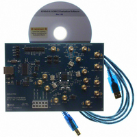
Manufacturer Part Number
AD9549/PCBZ
Description
BOARD EVALUATION FOR AD9549
Manufacturer
Analog Devices Inc
Datasheet
1.AD9549ABCPZ.pdf
(76 pages)
Specifications of AD9549/PCBZ
Main Purpose
Timing, Clock Generator
Embedded
No
Utilized Ic / Part
AD9549
Primary Attributes
2 Inputs, 2 Outputs, VCO
Secondary Attributes
CMOS, HSTL Output Logic, Graphical User Interface
Lead Free Status / RoHS Status
Lead free / RoHS Compliant


AD9549
Parameter
LOCK DETECTION
DIGITAL TIMING SPECIFICATIONS
SERIAL PORT TIMING SPECIFICATIONS
PROPAGATION DELAY
IO_UPDATE Pin Setup Time
Frequency Tuning Word Update,
Phase Lock Detector
Frequency Lock Detector
Time Required to Enter Power-Down
Time Required to Leave Power-Down
Reset Assert to High-Z Time
Reset Deassert to Low-Z Time
SCLK Clock Rate (1/t
SCLK Pulse Width High, t
SCLK Pulse Width Low, t
SDO/SDIO to SCLK Setup Time, t
SDO/SDIO to SCLK Hold Time, t
SCLK Falling Edge to Valid Data on
CSB to SCLK Setup Time, t
CSB to SCLK Hold Time, t
CSB Minimum Pulse Width High, t
IO_UPDATE Pin Hold Time
FDBK_IN to HSTL Output Driver
FDBK_IN to HSTL Output Driver with 2×
FDBK_IN to CMOS Output Driver
FDBK_IN Through S-Divider to CMOS
from SCLK Rising Edge of the Final Bit
Time Threshold Programming Range
Time Threshold Resolution
Lock Time Programming Range
Unlock Time Programming Range
Normalized Frequency Threshold
Normalized Frequency Threshold
Lock Time Programming Range
Unlock Time Programming Range
for S1 to S4 Configuration Pins
for S1 to S4 Configuration Pins
SDIO/SDO, t
Frequency Multiplier Enabled
Output Driver
IO_UPDATE Pin Rising Edge to DAC
Output
Programming Range
Programming Resolution
DV
CLK
)
LOW
HIGH
H
S
DH
DS
PWH
Min
0
32 × 10
192 ×
10
0
32 × 10
192 ×
10
8
8
1.93
1.9
1.34
−0.4
3
t
t
CLK
CLK
−9
−9
−9
−9
Typ
0.488
5 ×
10
15
18
60
30
25
2.8
7.3
8.0
8.6
60/fs
−13
Rev. D | Page 8 of 76
Max
2097
275
67 × 10
0.0021
275
67 × 10
50
11
−3
−3
Unit
μs
ps
sec
sec
sec
sec
µs
µs
ns
ns
MHz
ns
ns
ns
ns
ns
ns
ns
ns
sec
sec
ns
ns
ns
ns
ns
Test Conditions/Comments
FPFD_gain = 200
FPFD_gain = 200
In power-of-2 steps
In power-of-2 steps
FPFD_gain = 200; normalized to (f
Frequency Lock Detection
FPFD_gain = 200; normalized to (f
Frequency Lock Detection
In power-of-2 steps
In power-of-2 steps
Time from rising edge of RESET to high-Z on the S1,
S2, S3, and S4 configuration pins
Time from falling edge of RESET to low-Z on the S1, S2,
S3, and S4 configuration pins
Refer to
parameters, maximum SCLK rate for readback is
governed by t
Refer to
t
t
fs = system clock frequency in GHz
CLK
CLK
= period of SCLK in Hz
= period of SCLK in Hz
Figure 58
Figure 56
DV
for all write-related serial port
section for details
section for details
REF
REF
/R)
/R)
2
2
; see the
; see the
Related parts for AD9549/PCBZ
Image
Part Number
Description
Manufacturer
Datasheet
Request
R


Part Number:
Description:
±1.7g Dual-Axis IMEMS Accelerometer Evaluation Board
Manufacturer:
Analog Devices Inc
Datasheet:

Part Number:
Description:
Inertial Sensor Evaluation System
Manufacturer:
Analog Devices Inc
Datasheet:
Part Number:
Description:
Manufacturer:
Analog Devices Inc
Datasheet:
Part Number:
Description:
Manufacturer:
Analog Devices Inc
Datasheet:
Part Number:
Description:
Manufacturer:
Analog Devices Inc
Datasheet:
Part Number:
Description:
Manufacturer:
Analog Devices Inc
Datasheet:
Part Number:
Description:
Manufacturer:
Analog Devices Inc
Datasheet:
Part Number:
Description:
Manufacturer:
Analog Devices Inc
Datasheet:
Part Number:
Description:
Manufacturer:
Analog Devices Inc
Datasheet:
Part Number:
Description:
Manufacturer:
Analog Devices Inc
Datasheet:
Part Number:
Description:
Manufacturer:
Analog Devices Inc
Datasheet:
Part Number:
Description:
Manufacturer:
Analog Devices Inc
Datasheet: