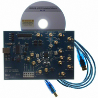
AD9549/PCBZ Analog Devices Inc, AD9549/PCBZ Datasheet - Page 28

AD9549/PCBZ
Manufacturer Part Number
AD9549/PCBZ
Description
BOARD EVALUATION FOR AD9549
Manufacturer
Analog Devices Inc
Datasheet
1.AD9549ABCPZ.pdf
(76 pages)
Specifications of AD9549/PCBZ
Main Purpose
Timing, Clock Generator
Embedded
No
Utilized Ic / Part
AD9549
Primary Attributes
2 Inputs, 2 Outputs, VCO
Secondary Attributes
CMOS, HSTL Output Logic, Graphical User Interface
Lead Free Status / RoHS Status
Lead free / RoHS Compliant
AD9549
Use of Line Card Mode to Eliminate Runt Pulses
When two references are not in exact phase alignment and
a transition is made from one to the other, it is possible that an
extra pulse may be generated. This depends on the relative edge
placement of the two references and the point in time that a switch-
over is initiated. To eliminate the extra pulse problem, an enable
line card mode bit is provided (Register 0x01C1, Bit 4). The line
card mode logic is shown in Figure 34. When the enable line card
bit is set to 0, reference switchover occurs on command without
consideration of the relative edge placement of the references.
This means that there is the possibility of an extra pulse. However,
when this bit is set to 1, the timing of the reference switchover is
executed conditionally, as shown in Figure 35.
Note that when the line card mode is enabled, the rising edges
of the alternate reference are used to clock a latch. The latch
holds off the actual transition until the next rising edge of the
alternate reference.
Figure 35 shows a timing diagram that demonstrates the difference
between reference switchover with the line card mode enabled
and disabled. If enabled, when the reference switchover logic is
given the command to switch to the alternate reference, an actual
transition does not occur until the next rising edge of the alter-
nate reference. This action eliminates the spurious pulse that can
occur when the line card mode is disabled.
FROM REFERENCE
SELECTION LOGIC
REFA_IN
REFB_IN
REFA IN
REFB IN
REF IN
REF IN
Figure 34. Reference Switchover Control Logic
Figure 35. Reference Switchover Timing
SELECT
1
1
1
REFA
1
0
1
0
1
2
LINE CARD
2
2
REF SELECTION STALLED UNTIL
ENABLE
NEXT RISING EDGE OF REFB
MODE
2
REFERENCE
SELECTED
3
0
1
SELECT REFB
Q
3
3
D
3
4
4
REF IN
FROM
REFERENCE
SELECTION
LOGIC
4
4
5
LINE CARD
DISABLED
ENABLED
MODE
Rev. D | Page 28 of 76
Effect of Reference Input Switchover on Output Clock
This section covers the transient behavior of the AD9549
during a clock switchover event. This is also applicable when
the AD9549 leaves holdover and reverts to being locked to
a reference input. There is no phase disturbance entering
holdover mode.
Switching reference inputs with different phases causes a transient
frequency disturbance at the output of the PLL. The magnitude
of this disturbance depends on the frequency of the reference
inputs, the magnitude of the phase offset between the two
references, and the digital PLL loop bandwidth.
Figure 36 shows the output phase as a function of time for a
reference switchover event. In this example, Reference A and
Reference B are both 30.72 MHz and have a 10 ns (102°) phase
offset. The digital PLL loop bandwidth is 0.2 Hz.
The frequency disturbance is the slope of the shift in Figure 36.
The maximum slope is 4.75 divisions in one second of time,
which gives the following transient frequency error, assuming
that the output is also 30.72 MHz:
The maximum frequency error for this transient is
To apply this to a general case, the designer should calculate the
maximum time difference between two reference edges that are
180° apart. The preceding calculation of the slope, m, becomes
0.5 Hz, not 0.292 Hz, for a phase shift of 180°. Next, the frequency
error must be scaled for the loop bandwidth used. The frequency
error for 1 kHz is 5000× greater than for 0.2 Hz, so the peak
frequency error for the preceding example of 102° is 47.4 ppm,
and 81.3 ppm for a 180° phase error between the reference inputs.
m
MaxFrequen
Figure 36. Output Phase vs. Time for a Reference Switchover
31
29
27
25
23
21
19
=
0
∆
∆
x
y
10ns DELTA @ 0.2Hz BANDWIDTH, 70° PHASE MARGIN
=
0.5
. 4
cyError
75
s 1
1.0
divs
REFERENCE SWITCHING:
=
1.5
=
TIME (s)
30
105
. 0
s 1
.
292
72
2.0
°
MHz
=
Hz
. 0
2.5
292
=
. 0
Hz
3.0
0095
3.5
ppm
4.0


