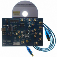
AD9549/PCBZ Analog Devices Inc, AD9549/PCBZ Datasheet - Page 25

AD9549/PCBZ
Manufacturer Part Number
AD9549/PCBZ
Description
BOARD EVALUATION FOR AD9549
Manufacturer
Analog Devices Inc
Datasheet
1.AD9549ABCPZ.pdf
(76 pages)
Specifications of AD9549/PCBZ
Main Purpose
Timing, Clock Generator
Embedded
No
Utilized Ic / Part
AD9549
Primary Attributes
2 Inputs, 2 Outputs, VCO
Secondary Attributes
CMOS, HSTL Output Logic, Graphical User Interface
Lead Free Status / RoHS Status
Lead free / RoHS Compliant
The phase lock detect signal is generated once the control logic
observes that the output of the comparator has been in the true
state for 2
Filter section for a description of the P-divider). When the phase
lock detect signal is asserted, it remains asserted until cleared
by an unlock event or by a device reset.
The duration of the lock detection process is programmable via
the phase lock watchdog timer bits. The interval is controlled by a
5-bit number, X (0 ≤ X ≤ 20). The absolute duration of the
phase lock detect interval is
Hysteresis in the phase lock detection process is controlled by
specifying the minimum duration that qualifies as an unlock
event. An unlock event is declared when the control logic
observes that the output of the comparator has been in the false
state for 2
phase lock detect signal has been asserted). Detection of an
unlock event clears the phase lock detect signal, and the phase
lock detection process is automatically restarted.
The time required to declare an unlock event is programmable
via the phase unlock watchdog timer bits. The interval is
controlled by a 3-bit number, Y (0 ≤ Y ≤ 7). The absolute
duration of the unlock detection interval is
PHASE ERROR
COMPARATOR
THRESHOLD
MAGNITUDE
SAMPLES
UNLOCK
t
t
UNLOCK
LOCK
TIMER
TIMER
(X = 3)
(Y = 1)
LOCK
f
f
R
S
x
Y + 1
/R
/P
0
periods of the P-divider clock (see the Digital Loop
=
periods of the P-divider clock (provided that the
=
2
X
f
2
S
P
Y
f
+
S
1
P
DETECTOR
P-DIVIDER
SAMPLES
CLOCK
PHASE
DIFFERENCER
REGISTERS
I/O
Figure 31. Lock/Unlock Detection Timing
FREQUENCY LOCK DETECT
Figure 30. Frequency Lock Detection
ABSOLUTE
VALUE
THRESHOLD
Rev. D | Page 25 of 76
COMPARATOR
DIGITAL
8
Figure 31 shows the basic timing relationship between the
reference signal at the input to the phase detector, the phase
error magnitude, the output of the comparator, and the output
of the phase lock detector. The example shown here assumes
that X = 3 and Y = 1.
Note that the phase and frequency lock detectors may erroneously
indicate phase/frequency lock while in holdover. Therefore, the
user should use the phase and frequency lock signals in conjunc-
tion with either the reference input valid or the holdover active
signals to indicate phase/frequency lock.
Frequency Lock Detection
Frequency lock detection is similar to phase lock detection, with
the exception that the difference between successive phase
samples is the source of information. A running difference of
the phase samples serves as a digital approximation to the time-
derivative of the phase samples, which is analogous to frequency.
The formula for the frequency lock detect threshold value
(FLDT) is
where f
the reference prescaler, and Δf is the maximum frequency
deviation of f
condition (Δf ≥ 0).
UNLOCK
TIMER
Y
FLDT
CONTROL LOGIC
3
4
R
is the frequency of the active reference, R is the value of
RESET
=
TIMER
R
LOCK
round
that is considered to indicate a frequency-locked
X
5
8
CLOSE
LOOP
∆
f
×
2
10
FREQUENCY
LOCK
DETECT
×
10
THRESHOLD
7
×
FPFD
LOCKED
_
Gain
AD9549
f
R
R
2


